
Introduction
A CCD is an imaging device that detects photons, converts them into photoelectrons and moves electrical charge. They are comprised of a silicon surface onto which an integrated circuit is etched. This etched surface forms an array of pixels which collect incoming photons, generating photoelectrons. These photoelectrons have a negative charge, so can be shifted along the sensor to readout registers where they can be amplified and converted into digital grey levels. This process is called charge transfer, as depicted in Figure 1(A,B). For more information on this process, visit our Fundamentals Behind Modern Scientific Cameras page.
When the electrons are shifted down the sensor to the readout register (Figure 1C), they are shifted horizontally off the register onto an output node (Figure 1D). They are then transferred to a capacitor, an amplifier, and analog-to-digital converter, and finally the imaging software in which the image is displayed.
An accurate image is created by maintaining the order in which the electrons are read out by the output node, determining their location on the sensor. However, this process has several limitations which can greatly slow down the process (i.e. the frame rate or frames per second) that a CCD can operate at:
• There is only one output node per sensor: Each pixel has to pass through this one node, amplified and digitized. This process introduces read noise to each pixel.
• Electrons will repel each other if transferred too quickly: This is prevented by limiting the speed at which electrons are transferred, however this further delays readout
• The entire sensor needs to be cleared of electrons before the next exposure to light and the next frame of an image: some CCDs require a mechanical shutter to block light so the sensor can be cleared, introducing slow-moving parts with a short lifetime.
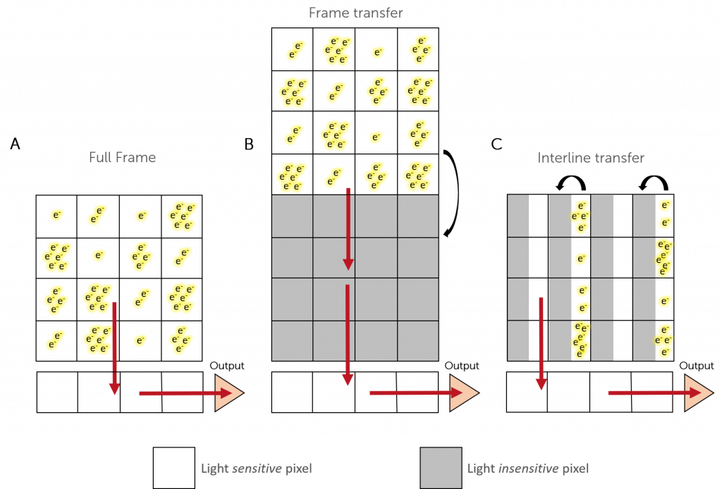
To try and minimize these speed limitations, several different CCD sensor formats have been designed to make the process more efficient and streamlined. The process shown in Figure 1 is called a full-frame CCD, however there are also frame-transfer and interline-transfer CCDs, as shown in Figure 2.
Full-Frame Transfer
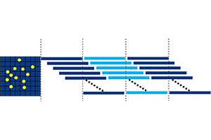
Full-frame transfer CCDs have a full, light sensitive pixel array onto which incoming photons are detected. The charge accumulated on the sensor must then be vertically transferred, in rows, to the output register to be readout. Once the charge from one row has been transferred to the output register, it must move horizontally to readout each pixel individually (Figure 2A).
Full-frame transfer CCDs are the simplest form of sensors and highly sensitive; however, they scan at a slow rate as each row needs to be readout individually, and the sensor needs to be completely cleared of electrons before another image can be acquired. They also can accumulate charge smearing, caused from light falling on the sensor during the transfer process, however this can be overcome through the use of a mechanical shutter.
Frame Transfer
Frame-transfer CCDs have a parallel register which is divided into the image collecting array, on which the images are focused, and the storage array (Figure 2B). Typically, both these arrays are identical in size, usually resulting in a sensor that is double in height to prevent any reduction in light sensitive sensor area. After the image array is exposed to light, the entire image is rapidly shifted to the storage array.
While the storage array is being read by the system electronics, the image array integrates charge for the next image. For this transfer system to work, there needs to be two sets of parallel register clocks that independently shift charge on either the image or storage array. This allows for continuous operation without a shutter at high frame rates. However, charge smearing can still occur with frame-transfer CCDs between the light-sensitive array and the masked array, but not to the extent of full-frame transfer CCDs.
Interline Transfer
Interline transfer CCDs have alternating parallel strips of light-sensitive and masked portions of the pixels (Figure 2C). These alternating strips allow for rapid shifting of any accumulated charge as soon as image acquisition is complete. As this process is so rapid, the likelihood of charge smear is removed, and images can be taken in quick succession.
However, as the masked are of each pixel makes each pixel effectively smaller, decreasing the sensitivity of the sensor. Microlens arrays can be used to overcome this, increasing the amount of light that can be captured for each active pixel.
Deep-Depletion CCDs
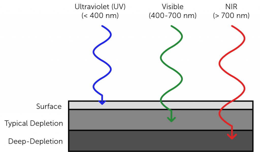
Silicon-based CCDs are optimized for photons in the visible wavelength range (400-700 nm). Wavelengths that are within the near infrared (NIR) range (>700 nm) are not able to be detected by traditional silicon CCDs as the longer the wavelength, the deeper within the silicon structure the photons travel before generating a signal charge.
However, thicker silicon sensors, called deep-depletion CCD sensors, are able to detect NIR wavelengths and higher energy x-rays as they provide enough material for the generation of a signal charge at these longer wavelengths, as shown in Figure 4. This makes deep-depletion CCDs optimal for applications that require both the visible and NIR spectrum.
HiRho CCDs
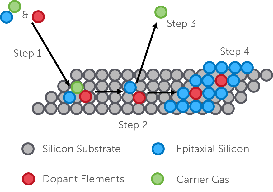
Standard and deep-depletion silicon sensors are typically comprised of a bulk silicon substrate onto which an epitaxial layer is grown. These epitaxial layers are incorporated into a device via a deposition process in which doped silicon is grown onto an existing bulk silicon substrate (Figure 5).
The silicon substrate and doped silicon layer will be either n- or p- type silicon. These types of silicon are formed when pure silicon is intentionally doped with different elements to control the electrical, structural and optical properties of the material.
N-type silicon is formed when the pure silicon is doped with arsenic or phosphorus. These elements have 5 electrons in their outer orbital, so are able to form 4 bonds within the silicon structure and still have a bond free to move any electric current. This makes n-type silicon negatively charged. P-type silicon is doped with boron or gallium, both of which have 3 electrons in their outer orbital. They therefore form “holes” as one electron in the outer orbital of a neighboring silicon atom has nothing to bind to, creating a positive charge. They are still able to conduct an electric current as they can accept electrons from neighboring atoms.
When creating a CCD semiconductor, the deposited epitaxial layer must be a different type to the silicon substrate. Therefore, an n-type epitaxial layer will be deposited onto a p-type silicon substrate, and vice versa. This produces high quality sensors, with moderate resistivity, that are relatively thin.
However, for high QE even further into the red region devices with an even thicker depletion are required. This deeper depletion is dictated by the operating voltages of the device and the resistivity of the substrate, with higher voltages and resistivity generating a thicker depletion region.
HiRho sensors are comprised of an epitaxial layer which is grown, via the deposition process, onto a very high resistivity bulk silicon substrate. These devices can also operate at higher voltages, meaning that these devices are able to provide thicker depletion regions within the silicon. This allows HiRho devices to detect wavelengths deeper into the red region, with >95% QE at 900 nm.
Summary
CCDs are silicon-based sensors comprised of a silicon substrate, and a deposited epitaxial layer. An integrated circuit it etched onto the silicon surface to make an array of pixels, which count the number of incoming photons and convert them to photoelectrons. These electrons are transferred down the sensor until they are readout and digitized to display an image on the imaging software.
There are various formats of CCD sensor which aim to streamline the process of photoelectron transfer: full-frame, frame and interline transfer. Full-frame utilizes the entire sensor for collection of photons, but has a much slower readout as all electrons must be cleared before a new image can be acquired.
Frame transfer takes advantage of a parallel register, making it twice the height, rapidly shift any detected photons onto a storage array without compromising on the size of the light sensitive area. However, these sensors are usually more expensive and susceptible to smearing artifacts.
Interline transfer uses alternating parallel strips, in which a portion of each pixel is masked to light, allowing for fast transfer without any charge smear. This however reduces the light sensitive area and makes the light collecting area of each pixel smaller.
Wavelengths >700 nm require deep-depletion or HiRho CCDs to be detected. As these sensors have a thicker depletion region, they are no longer transparent to NIR wavelengths and are therefore able to generate charge, detecting each NIR photon.
References
- Powell, M., VO2 Thin Films and Nanoparticles, from Chemical Vapour Deposition and Hydrothermal Synthesis, for Energy Efficient Applications, DOI: 10.13140/RG.2.2.35456.53762
Further Reading
EMCCD Sensors
Electron multiplying CCD (EMCCD) sensors are a variant of CCDs which capture a low number of photons and convert them into a high signal.
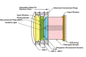
ICCD/emICCD Sensors
Intensified CCD (ICCD) sensors are another variant of CCDs but with the addition of an intensifier. This allows for nanosecond gating optimal for ultra-low exposure times.
sCMOS Sensors
sCMOS cameras provide low noise, alongside high speed, high quantum efficiency and high resolution. sCMOS sensors use parallelization to image at much higher speeds.