C. Martin de Sterke
University of Sydney, Nature Communications
Modular nonlinear hybrid plasmonic circuit
Introduction
Si photonics is a key technology and heavily researched area due to its broad applications from quantum computing to bio sensing. Testing and characterization of photonic structures requires sensitive, precise and quantitative imaging and spectroscopy solutions from visible to infrared wavelengths (Telecom wavelength).
Photonic integrated circuits are chip scale devices that perform complex optical functions and processes using light. As optical miniaturization and devices get more complex it can be practical to follow more modular design approaches for a combination of elements with different optical functions and research. As devices get more complex, design approaches with modular character are advantageous. Such devices also have to use design strategies that combines Si waveguides with plasmonic, metallic elements that are used to achieve optical functionality on PIC platforms, with high coupling efficiency.
Researchers around Prof. Martijn de Sterke from the University of Sydney (Australia) wrote in a recent article that so called “hybrid plasmonic waveguides containing a low-index buffer layer between the metal and the high-index waveguide” provide “a convenient interface for coupling between photonic and plasmonic waveguides.” Together with collaborators from Jena and Braunschweig (Germany) the researchers around Prof. de Sterke report on their efforts to build more complex circuits of these hybrid structures, using “multiple modular, function elements”.

The researchers created a plasmonic device that rotates the polarization of an incoming TE polarized, IR beam into a TM polarized beam that is converted into a visible output through non-linear, second harmonic generation. The device incorporates nanofocusing elements, which are sharp metallic tips that confine light to a ultra-small (nanometer sized volume) leading to giant electric field enhancements and thus more second harmonic light generation.
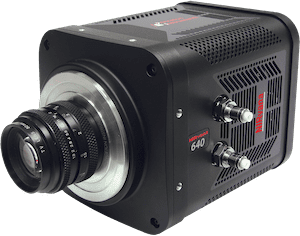
The processed, nano-structured devices are evaluated using microscopic imaging and spectroscopy. The microscope is coupled to a spectrograph operated with 2 cameras for detection. As the devices were designed for an input wavelength of 1320nm with SHG output at 660nm, the setup used a Teledyne Princeton Instruments NIRvana camera for SWIR light and PIXIS CCD camera for visible light detection and spectroscopy. The setup performs several measurement functions:
• Imaging monitors light scattering from the nanostructures on the devices, confirming the efficiency of polarization rotation and second harmonic generation with changing design dimensions.
• Spectroscopy characterizes the spectral response, for example comparison of the input light and output light spectrum confirms the SHG nature of the visible light.
• The SHG light is measured quantitatively to obtain the spectral conversion efficiency achieved.
The article shows how nanofocusing is achieved, as the SHG sharply increases for smaller metallic tips, and they discuss how the device efficiency could be further improved. According to this research the modular design approach can be practically applied to more complex devices and is compatible with CMOS processing techniques using Cu and Al as metals without degradation of device quality. The potential applications include “on-chip quantum photonics and spectroscopy, nonlinear and atomic scale sensing, and nanoscale THz sources and detectors”.


