Haiming Zhu
J. Chem. Phys
Introduction
Prof. Haiming Zhu and his research team at Zhejiang University in China investigate multiple aspects of 2D materials and van-der-Waals heterostructures involving their behavior when excited by light. Van-der-Waals heterostructures are layers of atomically thin 2D materials that can be stacked in specific orders to achieve desired device properties. They are studied around the world as this new class of devices can have physical properties and behavior that can’t be achieved with similar bulk structures.
Prof. Zhu’s group recently investigated the suitability of van-der-Waals heterostructures for efficient light harvesting and report on their experiments and findings in a new article in the Journal of Chemical Physics. Their findings are relevant for photovoltaics and opto-electronic devices that are traditionally bound by the 30% Shockley-Queisser limit for efficiency. However, in 2D materials this limit can be exceeded if high energetic or hot photo-excited charges can be extracted fast enough at the material interface of the device to not recombine either by light emission or nonradiative processes.

The researchers built van-der-Waals heterostructures from transition metal dichalcogenides MoTe2 and WS2, which are investigated using optical techniques, that are very common for the characterization and investigation of 2D materials. Prof. Zhu’s group uses photo-luminescence (PL) spectroscopy, absorption spectroscopy and transient pump-probe absorption spectroscopy for their experiments.
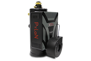
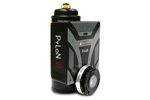
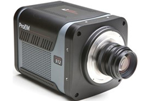
The setup for PL and absorption spectroscopy involves detection from the visible into IR wavelength covering a range from 2.1eV (590nm) to 0.9eV (1370nm) due to the broadband material characteristics. A Pylon-100 camera is used for efficient detection from visible to NIR and a Pylon-IR cryogenic InGaAs array for detection above 1000nm. For transient absorption spectroscopy a pump-probe setup is used pumping the samples with an ultrashort 35fs pulse and using a ProEM-1600 EMCCD camera for detection.
PL spectroscopy is used for the initial characterization of the materials and identifying the number of layers to find suitable samples for producing the stacked structures. By observing the behavior of the PL emission between the original and stacked layers the researchers identified changes to the electronic environment and interactions of charges when the materials are combined. For example a strong emission line of WS2 around 2eV is strongly suppressed in the stacked layer indicating the ultrafast charge transfer to MoTe2 layer. The transient absorption measurements then allows the researchers to reveal the details of the charge carrier behavior and what the mechanism for the charge transfer and its efficiency is for this particular structure.
In their conclusion the team notes that they could show effective charge transfer in the investigated structure, making these materials suitable for highly efficient devices. They note that their “findings […] enable fresh and exciting opportunities for designing extremely thin absorber and hot-carrier devices using 2D” van der Waals hetersostructures.