
Photon Conversion vs Anti-Reflection Coatings
The majority of camera sensors are silicon-based, such as CCD sensors. Although silicon-based sensors have high quantum efficiency (QE) in the visible wavelength range, they are much less sensitive to wavelengths in the ultraviolet (UV) range (100-400 nm). This is because UV light is only able to penetrate the first few layers of silicon, and because silicon is highly reflective reducing the conversion rate (and therefore QE) of UV wavelengths.
Two improvements can be made to silicon sensors to overcome these issues. The first is a UV photon conversion process, which downconverts (i.e. converts to a longer wavelength) UV light to blue/green light once it has interacted with the surface of the sensor. The other is an anti-reflective (AR) coating which reduces the reflectivity of silicon, improving the QE of the sensor in the UV range. However, both of these processes are only able to improve the QE between 200-450 nm, otherwise a physical enhancement process is used. This is because each of these UV improvement processes absorb any incident light below 200 nm. For wavelengths <250 nm, UV enhancement processes should be used.
UV Photon Conversion
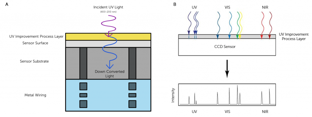
UV photons are only able to penetrate silicon at a short depth before being absorbed. This stops the UV photons from reaching the CCD channels (within the substrate), preventing these photons from being converted into photoelectrons, and therefore being readout.
UV photon conversion processes are able to down convert the UV photons so that they are able to penetrate the silicon more deeply before being absorbed, allowing them to be converted and then readout (Figure 1A). This allows the CCD sensor to be able to detect the incoming photon. When using a spectrometer (and an optical filter) the UV light will still be separated out and shown discretely as UV within a spectrum, even though the photon in the sensor channel has a longer wavelength (Figure 1B).
Photon Conversion Examples: Unichrome vs Metachrome
Unichrome is a phosphor-based conversion technology developed by Teledyne Princeton Instruments which is able to down convert any incident UV photons (below 400 nm) to blue light (~450 nm) allowing the sensor to detect the photon. It is a fluorescence material that is deposited directly on the bare silicon surface. It is excited by any incident UV light, and isotropically emits blue light into the sensor.
The thickness of Unichrome used on a silicon sensor is balanced so that the QE is enhanced, and the spatial resolution remains intact. Although it is opaque at wavelengths shorter than 450 nm, it is transparent at longer wavelengths, preventing it from altering any data collected. Maintaining spatial resolution is essential as the CCD sensor still needs to know the location of the UV excitation so that an accurate image can be ensured.
An alternative for Unichrome is Metachrome, a phosphor based Lumogen stack coating. This process works in the same way as Unichrome, however it downconverts any incident UV photons to green light (between 540 – 580 nm).
Unichrome has a broader, higher intensity peak than Metachrome, with >0.8 intensity over the 425-470 nm range (Figure 1A). In comparison, Metachrome has >0.8 intensity over the 515-540 nm range. However, Metachrome is able to improve etaloning (fringing) by 7.5x in comparison to Unichrome’s 1.5x improvement (Figure 2B,C). Therefore, if etaloning is a predominant limitation in data acquisition, Metachrome should be used.

Anti-Reflection Coatings
Every material has a refractive index, which determines the angle at which light is refracted within the material. It also determines how much light is reflected at the surface of the material, as well as the critical angle for total internal reflection. The refractive index is strongly dependent on the wavelength of incident light, with a smaller wavelength resulting in a larger refractive index. The refractive index can be described as:
Where c is the speed of light in a vacuum (~ 3 x 10⁵ km/s) and ν is the phase velocity of light within the chosen medium.
ν can be described as:
Where λ is the wavelength and T is a period of time, allowing the first equation to be rewritten as
This shows an inverse relationship between the refractive index and the wavelength of the medium
Refraction (i.e. the change of direction of light when it moves between mediums) is expressed using Snell’s Law:
n1 and θ1 are the refractive index and angle of incidence for one medium, with n2 and θ2 the corresponding parameters for the second medium. Figure 3 shows how incident light changes angle when propagating through two mediums with two different refractive indices.

Refraction describes how the light transmitted into the medium acts, however there is also incident light that is reflected. The reflectivity of a medium can be determined by Fresnel equations, which utilize Snell’s equation and the law of reflection (θi = θr where θi is the angle of incidence and θr is the angle of reflectance). Light which interacts with the normal of a medium (i.e. at a 90° angle), the Frensel equations can be reduced to:
Bare silicon (i.e. untreated silicon) has a high refractive index in comparison to air. This means that ~40% of incident light is reflected on the surface of silicon, with the remainder transmitted into the sensor. Not all of the light that is transmitted into the sensor will be converted into photoelectrons to be readout, further reducing the QE of the silicon sensor in the UV.
To overcome this an AR coating, comprised of a material with a different refractive index to silicon, is deposited onto the surface of the silicon-sensor to improve the quantity of UV light that is converted by the sensor (thus improving the QE). The thickness of this coating is chosen so that any wave reflected from the AR coating surface destructively interferes with any wave reflected from the silicon surface. This destructive interference results in a net zero reflectance of incident light on the silicon surface.
Summary
Improvements need to be made to silicon-based sensors to ensure that they have a high QE in the UV wavelength range. There are two ways that this can be done, either by UV photon conversion or via an anti-reflectance coating.
UV photon conversions works by downconverting any incident UV photons to longer wavelengths. At these longer wavelengths, the photons can penetrate to the silicon substrate, allowing for photoelectron conversion and signal generation.
Anti-reflective coatings reduce the reflectivity of the silicon by coating it in a material that has a lower refractive index, closer to that of air. This reduces the amount of incident light that is reflected, and increases that transmitted into the sensor, overall increasing the QE of the sensor. The thickness of the coating is also specifically chosen so that any reflected photons destructively interact with any reflected photons from the silicon, again further increasing the QE of the sensor.
Either of these improvements can be used for wavelengths over 200 nm. This is because shorter wavelengths are absorbed by the materials used within these improvements.
Further Reading
Quantum Efficiency
Quantum efficiency is the percentage of photons that an imaging device can convert into electrons. It is dependent on sensor material and wavelength of light being detected.
Camera Noise Sources
Noise within an image is caused by random variation of charge within the camera, resulting in changes to brightness or color.
Signal to Noise Ratio
The signal to noise ratio (SNR) is the relationship between the signal and the noise generated within the pixel.