
What is Ultraviolet (UV) Light?
Ultraviolet light spans over the wavelength range of 10-400 nm. It is used for many different applications, from material analysis to plasma diagnostics, with different sections of the wavelength range providing different application solutions. UV light can be separated into different wavelength ranges (see Figure 1):
- • Near Ultraviolet (NUV): 300 – 400 nm range (~3-4 eV)
- • Middle Ultraviolet (MUV): 200 – 300 nm range (~4-6 eV)
- • Far Ultraviolet (FUV): approximately 100 – 200 nm range (~6-10 eV)
- • Extreme Ultraviolet (EUV/XUV): 10-124 nm range (~10-124 eV)
EUV and MUV wavelength are often referred to as the vacuum ultraviolet range as they require a vacuum to be detected, due to the strong absorption of these photons by atmospheric oxygen. Alternatively, the system can be purged with a transparent gas, such as dry Nitrogen or Argon, in order to be detected (for wavelengths down to ~115 nm). These different UV sections require processed CCD sensors so that the photons can be detected.

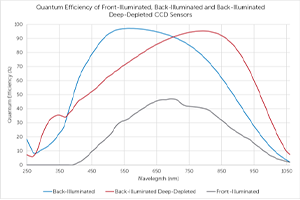
Traditional silicon-based CCDs have low quantum efficiency (QE) in the ultraviolet (UV) range. This is because UV light is absorbed readily by the CCD material, preventing the UV light to penetrate deep into the sensor (<2nm penetration of UV light). This shallow penetration depth means that the UV light is not detected by the pixel. Therefore, CCDs often require either a UV sensor enhancement or UV improvement process to enhance the QE in the 10-400 nm region.
UV Sensor Enhancements vs UV Improvement Processes: The Basics
UV sensor enhancements are physical alterations to a CCD sensor which allow for an increase in UV quantum efficiency. By passivating the back-illuminated CCD sensor, recombination of excess charge carriers can be reduced, increasing the QE of UV light. This enhancement is used on all UV sensors, with photons <200 nm relying solely on this process. Photons below this wavelength also require detection within a vacuum, as they are readily absorbed by the atmosphere, and are such described as the vacuum UV wavelength range (10 – 200 nm).
UV improvement processes are used in addition to UV sensor enhancements over the wavelength range 200 – 400 nm. There are two types of improvement processes, UV photon conversion and anti-reflectance coatings. UV photon conversion processes downconvert incident UV photons to photons with longer wavelengths so that they can penetrate deeper into the silicon and be detected. Anti-reflectance coatings have a refractive index closer to air than silicon, reducing silicon’s reflectivity. This decreases the percentage of photons reflected, increasing the overall QE.
EUV and FUV light require CCDs which have undergone a UV sensor enhancement in order to be detected by the sensor. MUV and NUV light, however, requires the sensor to have a UV improvement process as well as a UV sensor enhancement to allow detection of these photons.
UV Sensor Enhancement Fabrication
UV light is unable to penetrate deeply into silicon, with wavelengths <350 nm absorbing at depths <0.01 μm. This means that UV light interacts with the surface layers of the semiconductor. Therefore, physical and chemical changes to a silicon sensor are required to improve QE in the UV range.
The main way in silicon sensors are altered to improve the UV QE is via UV Enhancement. This involves additional back-thinning of the sensor, meaning that a shallow photon penetration depth can still result in a conversion to a photoelectron. This process is similar to traditional back-thinning, in which the p+ layer (doped layer formed from electron holes) is shallow at the surface of the sensor, but the UV Enhancement results in an even thinner p+ layer, bringing the potential peak as close to the sensor surface as possible. This minimizes any area of the surface which cannot absorb the UV photons, which is essential to improve QE for UV light.
The p+ layer is made shallow via ion implantation and UV activation. Ion implantation is a low-temperature process in which a solid target is bombarded with accelerated ions (from one element) to change the chemical or physical properties of the target. In this way, ion implantation is used to create the p+ layer, however, this layer needs to be passivated to reduce surface recombination. Passivation is a process in which the surface of a material is chemically altered to protect the material from the surrounding environment.
Traditionally, the etched surface of a semiconductor is fabricated so that any excess charge carries are recombined, with the positively charged holes within the semiconductor surface (from the p+ layer), removing excess photogenerated signals. As UV light is only able to penetrate the first few layers of the silicon semiconductor, they are most likely going to interact with the recombination layer. Therefore, the process of recombination must be minimized to allow UV photons to reach the silicon substrate and therefore be detected.
In order to passivate the p+ layer it must be activated by a UV laser pulse. The process of ion implantation and UV activation together melts a shallow surface layer, making the p+ layer thin enough for high UV QE.
UV sensor enhancements are the sole enhancement used on sensors to detect wavelengths <200 nm (i.e. UV improvement processes are not required).
UV Improvement Processes
UV improvement processes are comprised of different materials that are deposited onto the surface of the silicon sensor to improve the quantity of photons converted by the sensor. There are two types of improvement processes, UV photon conversion and anti-reflection coatings. Either of these improvement processes can be used alongside a UV enhanced sensor for a range of applications in the 400-200 nm range. Find out more about these processes in our article Photon Conversion and Anti-Reflection Coatings: Improving UV Sensitivity Above 200 nm.
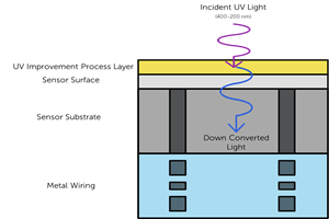
UV photon conversion down converts any incident UV photons into photons with longer wavelengths. As UV photons are only able to interact with the first few layers of a sensors, down conversion allows the photons to reach the sensor substrate, and therefore be converted into photoelectrons and readout. This drastically improves the quantum efficiency (QE) of the sensor within the UV wavelength range. This conversion occurs due to a fluorescent material, which covers the silicon surface and is excited by UV light, emitting photons of longer wavelengths.
Anti-reflection coatings cover the surface of the silicon in a material that has a different refractive index from the sensor. Silicon has a large refractive index in comparison to air, making it reflect ~40% of any incident photons. This relationship is strongly dependent on photon wavelength, with shorter wavelengths resulting in a larger refractive index. Therefore, bare silicon substrates reflect a high proportion of incident UV light, reducing the quantum efficiency (QE) of the sensor in the UV wavelength range. By adding an anti-reflection coatings, the refractive index of the sensor surface is reduced, resulting in less UV light reflected and therefore a higher QE.
What Applications Utilize UV Wavelengths?
There are a wide variety of applications that utilize UV wavelengths, with different subsections requiring different sensors to be able to investigate each application optimally. The following section looks at two applications which utilize UV enhancements and UV improvement processes for VUV wavelengths and NUV/MUV wavelengths respectively.
Plasma Characterization: VUV Wavelengths
Plasma is the fourth state of matter and is an ionized gas consisting of charged ions, electrons and particles. These components exist in an excited state, due to the high energy of the plasma needed to maintain ionization. When the particles, ions and electrons relax, electromagnetic radiation of various wavelengths is emitted. Characterizing this emission provides insight into plasma properties.
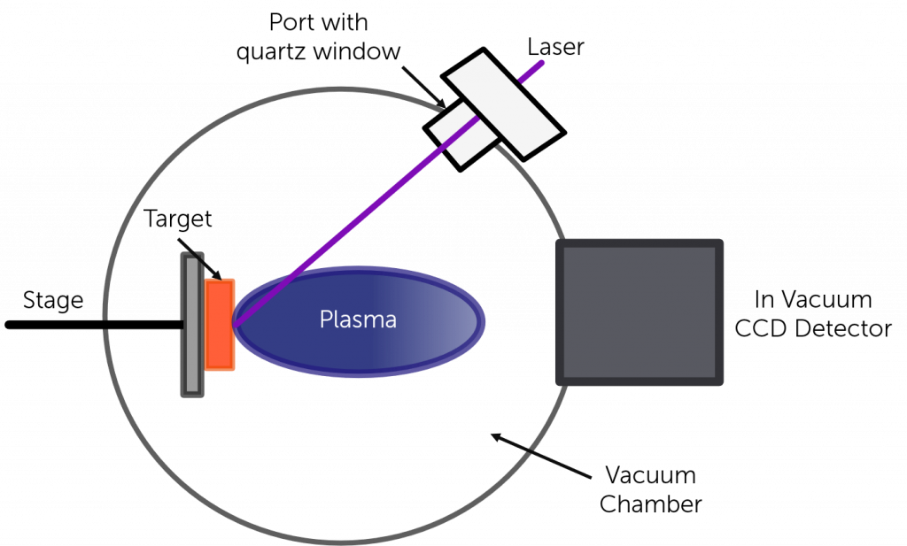
One way of forming a plasma is to focus a high-powered pulsed laser onto a solid target, as shown in Figure 2. Information about the target’s composition can then be established from the wavelength emission of the plasma. If the target is made up of rare earth elements, or any neighboring metal elements, VUV radiation is emitted. This is usually most intense between 4-30 nm (in the EUV range) however it can extend to the FUV range.
Analysis of emitted VUV radiation can be used to determine the properties of the plasma, such as electron density and electron temperature. As these plasma properties are determined by the composition of the target, VUV radiation can be used to provide insight into target chemistry. All VUV radiation is below 200 nm, therefore a camera with a UV enhanced sensor is required to be able to detect the emitted photons.
As laser-induced plasmas rely on a high-powered pulsed laser, they require a camera with fast readout speeds to be able to capture information from each pulse. They also rely on camera triggering to separate the large laser signal from the plasma signal. The SOPHIA-XO has both high readout speeds and triggering support which allows for plasma detection without interference from the laser light, at ultrafast speeds.
Materials Analysis: NUV/MUV Wavelengths
Materials analysis is a common application which utilizes the NUV/MUV wavelength. As UV light is reflected by many materials, it can be used to characterize surface topography without penetrating or destroying a material.
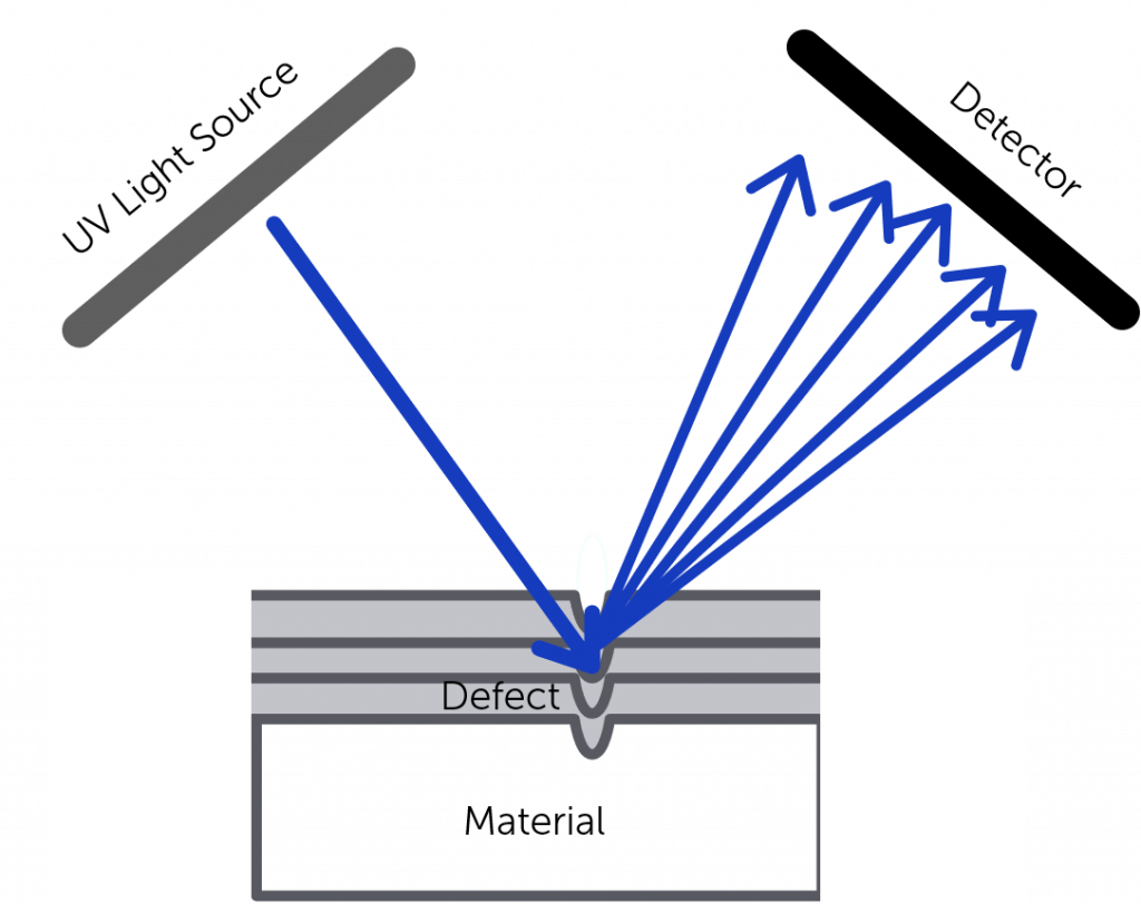
Both NUVs and MUVs have shorter wavelengths than visible/infrared light so are able to be scattered by very small surface features. This phenomenon is utilized in reflected-UV imaging to detected small defects on a material’s surface, for example small scratches not visible to the human eye (Figure 3). This technique is used within automated systems to detect defects on the surface of optics (i.e. windows or lenses) to ensure quality of product.
MUVs can also be used to look for defects on semiconductors. Integrated circuits, used within sensors, and computers among many other things, rely on photolithography for fabrication. Photolithography is a process which transfers patterns onto the surface of semiconductors. The process relies on a photomask which often has submicron features. MUV is the optimal wavelength range to detect any defects on these photomasks, as well as quality checking the bare silicon surface. This is advantageous as it ensures high quality production while minimizing product waste.
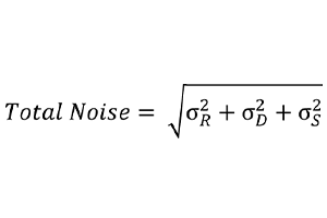
NUVs and MUVs cover a short wavelength range, so require high sensitivity between 3-6 eV (200-400 nm). As they are used predominately for defect detection, a sensor with high spatial resolution is essential, alongside low noise to prevent any artifacts. For example, the SOPHIA-XO is a CCD camera with high sensitivity across the entire UV range. It has low read and dark noise, optimal for defect detection using reflected-UV imaging.
An alternative to CCD technology is the sCMOS, which has lower read noise and a larger field of view, with higher frame rates than a CCD sensor. The KURO sCMOS camera has high QE in the MUV wavelength region, making it an alternative for semiconductor defect analysis. As it has a lower read noise and larger field of view, the KURO is able to detect defects within the MUV range while minimizing the appearance of artifacts.
Summary
The UV wavelengths range spans from 400 – 10 nm, with multiple subsections all used for various applications. These wavelength subranges all require different technology to achieve optimal performance.
UV sensor enhancements are physical and chemical alterations to a CCD sensor which allow for an increase in UV quantum efficiency. They are used for UV sensors that are detecting photons <200 nm. These photons are also detected within a vacuum to prevent atmospheric absorption.
UV improvement processes are for photons within the 400 – 200 nm range and are used alongside UV sensor enhancements. Both UV photon conversion and anti-reflectance coatings can be used, to either downconvert the UV photons or to reduce the reflectance of the silicon sensor. Both processes increase the quantum efficiency of the sensor.
Altered sensors are essential for applications which rely on UV detection. Plasma diagnostics, especially plasmas created from high-powered pulsed lasers, rely on the detection of VUV light. This light can be analysed to characterize the chemistry of the target material. VUV is also used within astrophysics, to understand plasmas created from our Sun. Stellar coronas and solar flares have strong emission lines in the VUV, so by detecting and characterizing VUV emission, more can be learnt about these dynamic events from the Sun.
NUV and MUV wavelengths are important within quality control and are commonly used to find defects on both optical equipment and semiconductors. Due to their short wavelengths, NUV/MUV are scattered by smaller defects more than visible/infrared light, allowing submicron alterations to be imaged. This increases the quality of product produced, as it can be implemented throughout the fabrication process, and reduces the amount of product waste produced.
Further Reading
Improving UV Sensitivity Above 200 nm
There are two processes which can be used to enhance UV sensitivity for wavelengths >200 nm: UV photon conversion, and anti-reflection coatings.
Quantum Efficiency
Quantum efficiency is the percentage of photons that an imaging device can convert into electrons. It is dependent on sensor material and wavelength of light being detected.
Camera Noise Sources
Noise within an image is caused by random variation of charge within the camera, resulting in changes to brightness or color.