
Introduction
Complementary metal-oxide-semiconductor (CMOS) sensors are a technology that has been around since the 1990s. Early CMOS cameras were competing with the more mature CCD technology, but over the 1990s and early 2000s CMOS sensor technology improved to the point where CCD technology was overtaken to become the sensor of choice for consumer digital cameras. This technology was then improved further still to fulfil the higher requirements essential for scientific imaging.
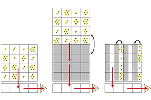
CMOS sensor technology differs from CCD sensors as instead of having all sensor pixels fed through one output node, one amplifier and one analog-to-digital converter (ADC) as with a CCD sensor, CMOS sensors work in parallel by having a miniaturized capacitor and amplifier on every pixel, and an ADC for every column (as shown in Figure 1). Each ADC acts simultaneously, reading out entire columns rather than individual pixels of the whole sensor. This makes the process much faster and requires 100x less power than CCD sensor architecture.

sCMOS Technology
In 2009, scientific CMOS (sCMOS) technology was launched, with sCMOS cameras being commercially available in 2010-11. sCMOS cameras are able to provide low noise, high speed, and a large field of view, making sCMOS cameras ideal for a wide range of applications, from astronomy to microscopy.
Rolling Shutter and Global Mode
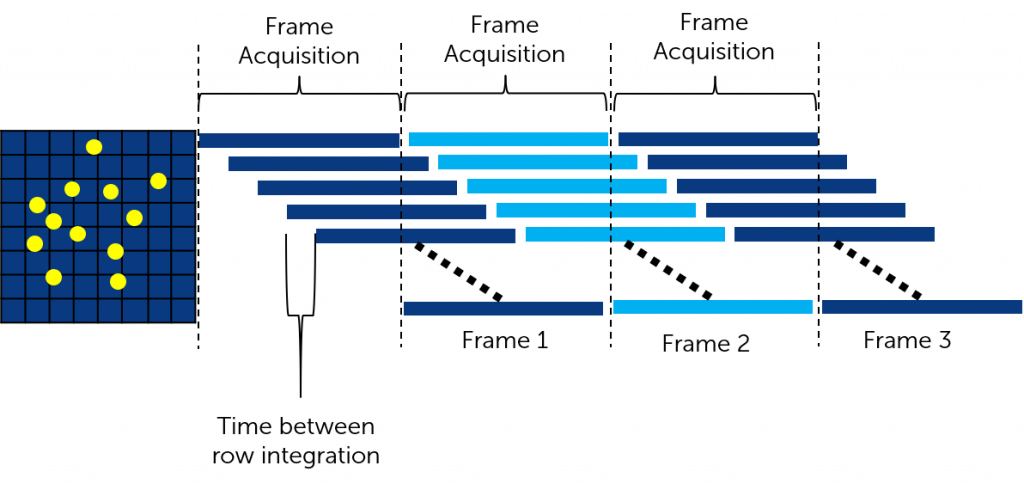
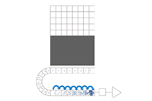
sCMOS sensors differ from CCD sensors as they typically have a rolling shutter. Image acquisition begins at the top of the sensor and works its way down, row by row. This allows the sensor to acquire images at much higher framerates with much lower read noise. The speed of an sCMOS camera directly relates to the number of rows, and the row time (i.e. the time between acquisition of one row and another).
Rolling shutters switch “on” and “off” by clearing the charge that is already within one row and measuring any new incident photons. This allows for an overlap between the acquisition of the current pixel row of a frame (which is acquiring an image), and the lower pixel rows of the previous frame (of an image being readout) (Figure 2).
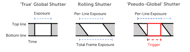
Some sCMOS sensors can be used in a pseudo-global shutter mode for zero distortion and applications involving hardware changes between frames, such as sequential dual-channel acquisition. This pseudo-global shutter takes advantage of controlling the triggering of the light source. To create this global shutter the camera needs to activate the rolling shutter in dark conditions. Then by triggering the light source and stopping the light at the same time as stopping the camera an area of the array can be illuminated simultaneously, just as a global shutter (as shown in Figure 3).
CCD vs sCMOS
The differences in CCD and sCMOS sensor architecture provide both advantages and disadvantages. Some of the advantages of sCMOS technology over CCD technology are as follows:
- Low read noise: sCMOS features read noises ~1 e- compared to 5-6 e- from CCDs. To understand the role of lowering read noise and improving sensitivity, click here.
- High speeds: sCMOS can achieve up to 100s fps compared to ~20 fps from CCDs. This is because each column has an ADC associated so has a fraction of the data to process.
- Large field of view: sCMOS sensors range cfrom 19-29 mm diagonal, compared to 11 – 16 mm from CCDs
- Power efficiency: sCMOS uses 100x less power than CCDs due to parallelization
Although sCMOS technology is advantageous to CCD technology in a number of ways, it does have some disadvantages:
- Increased temporal and fixed-pattern noise: as each pixel is readout individually more temporal and fixed-pattern noise is introduced. sCMOS sensors have more active readout areas than CCDs, which causes an increase in these noise sources. This can be reduced by careful electronic design and calibration by camera companies.
- Rolling shutter artifacts: sCMOS sensors can use a rolling shutter to acquire images, however if dynamic objects in the image are sufficiently fast enough to move on a similar timescale to the roll of the shutter, distortion effects can be introduced. Staggered readout between top row of the sensor and bottom row can also cause image artifacts and lost information, and significantly increases effective minimum exposure times for some applications.
Back-Illuminated sCMOS
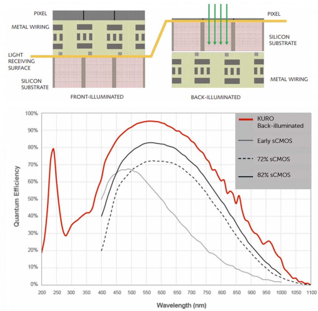
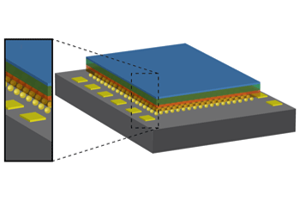
Some early sCMOS sensors had issues with background quality and noise, limiting the use of CMOS for more demanding applications. To overcome this, higher sensitivity was required to improve the technology. In 2016, back-illuminated sCMOS was created, offering a peak quantum efficiency (QE) of 95% without compromising pixel size, while also improvements were made to background quality. Figure 4 shows a diagram of back-illuminated sCMOS technology, alongside a QE curve indicating the difference between early sCMOS and back-illuminated sCMOS.
Summary
sCMOS sensors take advantage of active circuit integration into individual pixels. This allows each pixel to be read out individually. There is also an analog-to-digital converter attached to each column, allowing much higher frame rates while still maintaining low read noise, large field of view and high power efficiency.
Although there is an increase in temporal noise and fixed-pattern noise due to the increase in active circuits on the sensor, sCMOS technology is still advantageous from a wide range of applications.
Further Reading
CCD Sensors
CCD sensors are silicon based semiconductors which capture photons and covert them into photoelectrons. This is converted into a digital signal and read out by the camera.
EMCCD Sensors
Electron multiplying CCD (EMCCD) sensors are a variant of CCDs which capture a low number of photons and convert them into a high signal.
InGaAs Sensors
InGaAs focal plane array sensors are semiconductors which are optimized for shortwave near-infrared wavelengths (900 – 1700 nm).