
Introduction
Quantum efficiency (QE) is the percentage of incident photons that an imaging device can convert into electrons. For example, if a sensor had 75% QE and was exposed to 100 photons, it would be able to convert to 75 electrons of signal.
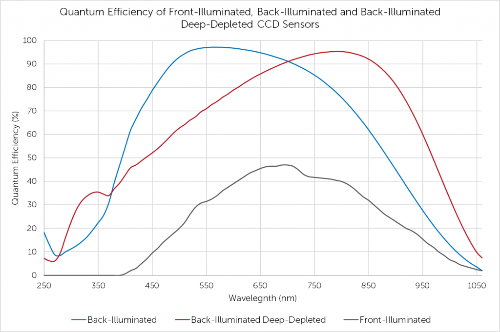
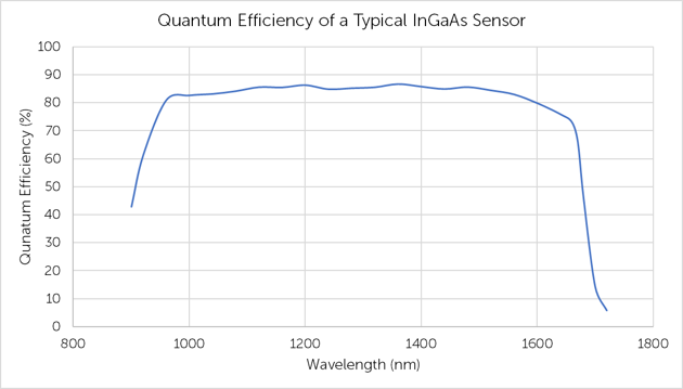
The QE is different for each sensor technology, with high end scientific sensors reaching 95% QE. However, it is determined by the wavelength of light being detected and the semiconductor material. Figure 1 shows the difference in QE between a back-illuminated silicon CCD sensor and an InGaAs sensor.

For CCD, EMCCD, (em)ICCD and sCMOS technology, 95% QE is possible within certain wavelength ranges, but photons in the near-red and ultraviolet regions of the visible spectrum have lower QE and therefore the sensor would be less effective. To improve QE in these regions, deep-depleted sensors and coated sensors have been developed, which increase the QE.
Silicon Sensors
Majority of scientific sensors are made of silicon. As QE is material dependent, it is important to look at the properties of this element and how it interacts with light.
In the high-purity crystalline form, neighboring silicon atoms are covalently bonded to one another. Energy greater than the band gap energy is required to break these bonds to create an electron/hole pair (~1.1 eV). The wavelength of incoming light and photon absorption depth are directly related; the shorter the wavelength, the shorter the penetration depth into the silicon.
Deep-depleted silicon sensors are thicker than traditional silicon sensors so are able to detect longer wavelength light (i.e. > 700 nm, NIR). The penetration depth of NIR light within silicon is deeper than a typical silicon sensor, so without deep-depletion the silicon sensor is effectively transparent to the incident NIR light. Deep-depleted silicon sensors can provide a QE of >90% between 700 – 850 nm in comparison to >60% with traditional silicon sensors, as shown in Figure 2.
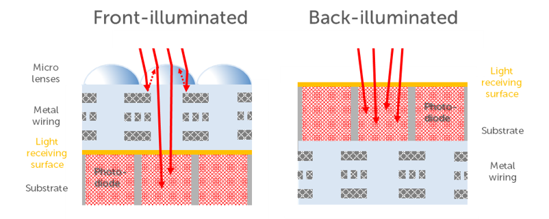
To further improve QE, the orientation of the sensor within the device can be altered with devices either being front- or back-illuminated (see Figure 2). The incident light of a front-illuminated device typically enters the sensor through the gates of the parallel register. These gates are made of very thin polysilicon, which at long wavelengths is reasonably transparent, however becomes opaque at wavelengths shorter than 400 nm. Therefore, at short wavelengths, gate structure attenuates incoming light.
If a silicon sensor is uniformly thinned, an image can be focused on the back end of the sensor where there is no gate structure. See Figure 3 for a comparison. As there is no light limitation from the gate structure, back-illuminated devices exhibit high sensitivity to light, making QE of 95% possible.
InGaAs Sensor
Semiconductors will only detect photons if they have a higher energy, or shorter wavelength, than the bandgap energy of the material. InGaAs sensors are semiconductors made of an alloy of InAs and GaAs, and traditional InGaAs sensors have a ratio of x:1-x of InAs:GaAs. As InGaAs is not a naturally occurring material, a single crystal has to be grown on an InP substrate.
InGaAs sensors usually have a lower band gap energy than silicon, meaning that they are able to detect longer wavelengths such as the shortwave infrared (SWIR) region (900-1700 nm). Therefore, InGaAs cameras can have a QE >80% over the 950-1600 nm region. Figure 4 shows the QE curve of a typical InGaAs sensor. By increasing the concentration of InAs within the single crystal, the cut off wavelength can be extended to 2600 nm.
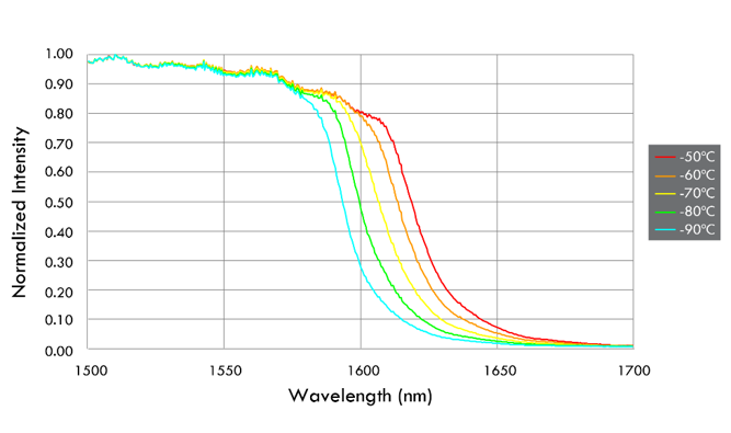
Although InGaAs cameras have high QE over the 900 – 1700 nm range, the far-end wavelength cut off decreases as the device is cooled. This typically shifts by 8 nm for every 10oC of cooling. This means that it is important to maximize photon throughput into the device, however this shift in far-end cut off can be advantageous as it allows the sensor to act as a “tunable” lowpass filter. Figure 5 shows how the far-end cut off changes with temperature decrease.
Summary
QE is the measure of how effective a device is at converting incident photons into electrons. Not only is the QE wavelength dependent, it is also dependent on the sensor material.
A sensor will detect an incident photon if the energy is higher than that of the semiconductors band gap energy. This is why silicon has a 95% QE between 500-600 nm but has lower QE for longer infrared/shorter violet wavelengths, yet InGaAs has a high QE over the SWIR range (900 – 1700 nm), and not the visible region or the mid-infrared wavelength range (>1700 nm).
Further Reading
Camera Noise Sources
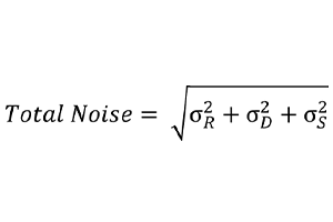
Noise within an image is caused by random variation of charge within the camera, resulting in changes to brightness or color.

Signal to Noise Ratio
The signal to noise ratio (SNR) is the relationship between the signal and the noise generated within the pixel.
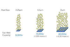
Full Well Capacity
Full well capacity is the amount of charge that can be stored within a pixel before saturation. At this point the well is full, no more charge can be stored.