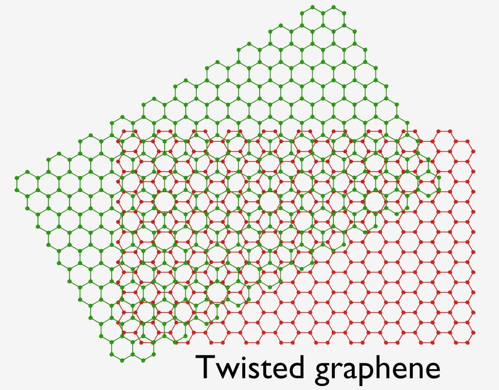
Raman spectroscopy has always been one of the most important measurement techniques for the characterization of 2D materials such as graphene, hexagonal boron nitride or transition metal dichalcogenides (TMDs). Analyzing their Raman spectrum reveals information on the number of layers, charge doping or stress and strain states. 2D materials can also be readily stacked into more complex structures. These so-called van der Waals heterostructures possess new physical properties and are fundamental for building new optoelectronic devices from 2D materials. It has been shown that not only the order of materials in the heterostructures is important to consider, but also their relative crystal orientation and the physical properties of so called twisted materials where the lattice of one layer is rotated relative to the layer below can change significantly.
Liam McDonnell and David Smith from the University of Southampton, UK and their coworkers are interested the physics of twisted van der Waals heterostructures. They use resonance Raman scattering to reveal interesting physics in TMD layers of MoSe2 and WSe2 and to characterize interactions between layers. In resonance Raman spectroscopy the excitation energy of the laser is brought in or close to resonance with the transition energy between electronic energy levels. The resonance effect typically leads to a massive increase in the Raman scattering signal which is often selective so only some Raman lines are enhanced. In TMDs resonance Raman has already been shown to be a probe of dark exciton states that are invisible in PL spectra, but couple to vibrational phonon modes.
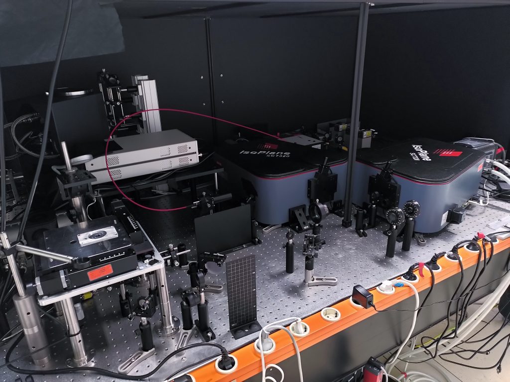
In their recent article the researchers show that resonance Raman is a good tool to measure interactions between the TMD layers. For excitation of Raman spectra they use a tunable Ti:Sapph (1.24eV -1.77eV) and dye laser (1.74eV – 2.27eV) while controlling the light polarization which helps to eliminate unwanted luminescence signal from the sample. The Raman signal is analyzed in a TriVista triple stage spectrograph. The multi-stage system works particularly well for resonance Raman experiments as they can be adjusted for changing excitation laser wavelength without use of external filters that would be designed for use with a single laser excitation wavelength. They also allow observation of signals at energies <100cm-1 which are important for studying interlayer interactions of TMDs, but can’t be observe with standard Raman filters.
When scanning the excitation energy across resonance of an intra layer exciton the researcher observe spectral lines that can only be explained by hybridization of intra and interlayer exciton states. They can show that resonance Raman is a good tool to characterize the interactions and quantify the hybridization properties. Moreover, the interaction is dependent on the twisting angle between the layers. As a result, the researchers hope that their results will lead to new ways of designing optoelectronic devices of 2D materials. They also see potential applications in quantum technology and quantum information processing where hybridized excitons could be basis for q-bit states.
Scientists around Prof. Alexander Högele from the Center for NanoScience and Center for Quantum Science and Technology at the Ludwig-Maximilians-University in Munich, Germany published an article about a new experimental setup for very sensitive cavity quantum electrodynamics measurements in closed cycle cryostats. They demonstrate the effectiveness of their passive and active vibration control by measuring strong coupling of a single layer of the transition metal dichalcogenide (TMD) WSe2 to an optical cavity.
Solid state quantum materials such as quantum dots, TMDs and rare earth ions are promising platforms for applications of quantum physics for computation, sensing and information processing. The researchers describe that these materials have to be cooled to cryogenic temperatures to reduce environment noise, however Helium that has traditionally been used is expensive and limited. The challenge of closed cycle systems are vibrations that are of the order of 10 micro-meter but need to be closer to 40 pico-meter to be useful for cavity QED experiments. The new experimental system at the University of Munich has a series of passive vibration control mechanisms, but also allows for active control receiving feedback through light reflection and interference in the optical cavity over a 100kHz bandwidth.
The setup is tested on a TMD monolayer of WSe2, encapsulated in 2 sheets of hexagonal boron nitride. The cavity is built from a concave fiber mirror and the substrate of the sample. For spectroscopic measurements of the sample the researchers use a high resolution SpectraPro spectrograph with 750mm focal length and detection using a liquid nitrogen cooled camera. The spectra show the exciton resonance around 1.723eV. The cavity is brought in resonance with the exciton (moving the fiber from 50μm distance to 2.9μm distance) while measuring the transmission spectra of a super continuum light source. Strong coupling between the photon field and the TMD is visible as an anti-crossing of the transmission signal which is a basic signature of coupled quantum oscillators.
After this successful demonstration the researchers plan to apply their experimental setup to further measurements on a wide range of quantum materials, single photon sources and qubit materials. They think that the already excellent vibration isolation can be improved even further in the future.
As the COVID-19 pandemic of 2020 and 2021 has shown, reliable, fast and cost effective detection of viral components and diagnostics is an important factor in management and mitigation of disease effects and spread. While PCR tests are the gold standard for testing they are relatively slow to process and resource intensive according to Deborah Crittenden, Mark Waterland and their team of researchers from University of Canterbury and Massey University (New Zealand). In a recent publication in ACS Omega they write that “it has been widely recognized that optical and/or electronic sensing technologies may hold the key to the development of rapid, high throughput, easy-to-use, point-of-care diagnostics.”
A challenge for these measurement techniques is that they need to achieve sensitivity to detect concentration in the fM range which represents a biologically and practically relevant value. The researchers implement 3 photonics based measurements systems for measurement of Covid-19 genetic signatures including biolayer interferometry and surface plasmon resonance, but the most sensitive technique studied was surface enhanced Raman spectroscopy (SERS). SERS enhances the vibrational Raman spectra of molecules in the presence of metallic nanoparticles.
To achieve high sensitivity the team functionalizes the surface of Ag nano particles with DNA aptamers that bind specifically to the CoV-SARS-2 spike proteins. Using Raman spectroscopy they observe changes in the aptamer Raman spectrum before and after binding of the viral components.
The SERS spectra are recorded by excitation with a 532nm laser and measuring the spectra (after filtering out laser light using a longpass edge filter) with anIsoplane-81 spectrograph, which allows for data collection with high resolution and sensitivity besides its small form factor.
The researchers then identify specific Raman bands that are attributed to N-H and C-H stretching vibrations and analysis including principal component analysis reveals a characteristic reduction of intensity in these bands in the presence of the spike protein. The results show that the applied SERS technique allows detection down to subfemtomolar concentrations. Moreover this method has high speed and sensitivity that make it a good building block for the development of rapid diagnostic instruments. Future public health challenge might see techniques like SERS applied on a large scale allowing for faster and better informed decisions to prevent large scale viral outbreaks.
Real-Space and Fourier Imaging and Spectroscopy of NIR Emission from SWCNTsCustomer Stories
Prof. Jana Zaumseil
Heidelberg University,Germany
Background
The group of Prof. Jana Zaumseil at Heidelberg University in Germany investigates novel semiconducting materials with focus on charge transport and application in optoelectronic devices. One research focus of the group is to build and investigate devices based on single-walled carbon nanotubes (SWCNT), one-dimensional structures that can be conceptualized as rolled-up sheets of graphene. In contrast to graphene, nanotubes can be metallic or semiconducting depending on their roll-up vector. By polymer-sorting, the different geometries can be selected. The 1D nature of the nanotubes leads to exceptionally strong bound states between electrons and holes that produce room-temperature stable excitons featuring narrow emission in the NIR. Using chemical functionalization, luminescent quantum defects can be introduced into nanotubes to tune the emission into wavelength regions relevant for telecom application or generate single-photon emission at room-temperature.
This makes nanotubes a promising material for novel optoelectronic devices such as ultrafast transistors, on chip photodetectors or potentially lasers. The group implements new device designs and proves their concept of operation. Jan Lüttgens, a doctoral student and scientist in the lab says that “one interesting aspect of my work is that we can make real devices ourselves to prove their principle of operation and test these concepts in the lab.”
One such concept, that is implemented in his experiments, is realized by embedding nanotubes in photonic structures, such as Fabry-Pérot cavities or plasmonic crystals which enhance their coupling to the electromagnetic field. Under the right conditions the device can be brought into the strong light-matter coupling regime which creates new hybrid states called exciton-polaritons. The strong coupling regime requires an optimized device design and can be tuned by contacting the nanotubes electrically to suppress excitations in the material or to pump the new hybrid-states electrically or even create charged-light-matter particles. Strong coupling between nanotubes and a cavity can also be used to fabricate photodiodes that can absorb light far-beyond the intrinsic nanotube band gap.
Challenge
An indicator for the presence of strong coupling between the nanotube states and the electromagnetic field is a characteristic mode splitting at the exciton energy in reflectivity and emission. For efficient observation of the mode structure the lab uses a technique called Fourier imaging spectroscopy. By inserting an additional lens into the beam path the cavity mode structure can be resolved in momentum and energy simultaneously by one-shot measurements. Compared to scanning based techniques it increases the measurement efficiency by reducing the acquisition time using a two-dimensional detector. Furthermore, tomography of the mode structure can be achieved by simply shifting the Fourier image relative to the detector. For NIR (or SWIR) emitters, this requires cameras which are sensitive in the wavelength range between 1-1.7μm.
However, NIR emitters usually suffer from low photoluminesence quantum yields and low dimensional materials additionally exhibit saturation effects at comparably low excitation powers. Working in the linear regime, therefore, requires low thermal noise detectors, to enable long integration times.
“In the NIR, the emission efficiency of materials drops drastically, so it is good to have low thermal noise.”
Solution
The Fourier Imaging setup of the Zaumseil group uses a NIRvana 640 camera and Isoplane spectrograph to enhance the capability for detection of the low light emission from nanotube devices and single tube samples. The two-dimensional InGaAs detector of the NIRvana camera with high quantum efficiency in the NIR, enables such experiments. The sensor of the camera is thermoelectrically cooled to -85⁰C to reduce the dark current on the sensor and an integrated cold shield system limits the influence of thermal background radiation on measurements. This makes the NIRvana 640 ideal for measurements of the weak signals that can require several seconds or more of integration time, combined with imaging capabilities of 2D detector array
The Isoplane spectrograph is designed to eliminate astigmatism and minimize optical aberrations that could distort the spectral images in the focal plane. Such a design increases the quality of spectral data across the whole focal plane of the spectrograph, which improves measurements such as Fourier Imaging Spectroscopy that use a large or even the whole sensor area of the camera.
Transition Metal Dichalcogenides are semiconductor materials that build single atom thin layers. They are heavily researched two dimensional materials and have been discovered to be useful for nanophotonic applications either on their own or combined in stacks with other 2D materials (so called van-der-Waals heterostructures). Many experiments investigate their behavior in combination with plasmonic and cavity nanostructures. Such devices allow investigation of interesting physics and are building blocks for components of photonic and quantum devices.
A new publication by a research collaboration around Prof. Tian Jiang and Prof. Lei Shi in China is reporting on their experiments combining monolayers of Tungsten diselenide with photonic crystal structures. Such nanostructures have a strong influence on energy as well as direction of light emission
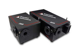
Energy-momentum spectroscopy is a perfect tool to observe the properties of these devices. This technique is equivalent to Fourier plane imaging in microscopy where instead of the direct image of the sample, the backfocal plane of the objective is observed revealing the direction of light emission. If this image is projected on the entrance slit plane of a spectrograph the relationship between light wavelength and its momentum can be directly observed. In the reported experiment the energy-momentum spectroscopy system is built around an Isoplane-320 spectrograph combined with a PIXIS 400 camera. Aberration corrected systems are perfectly suited for these measurements as important information is observed across the whole image sensor.
The researchers report that their energy momentum measurements reveal strong coupling in their device which allows them to study fundamental physics as well as show the potential of this material for applications in nanophotonic devices in the future.
Researchers from France have been using the FERGIE system (a previous version of the IsoPlane 81) to characterize materials used for optical fibers. While it is well known that optical fibers are commonly used for the transmission of information through fiber optic cables, they have found various other applications that they aid. For example, fiber optics can be used in creating high power optical fiber lasers as well as elements in new sensors for environment parameters like temperature. In particular, these sensors can also be used in harsh radiative environments (earth or spacebound). The radiation can create defects in the fibers that lead to so called color centers that sensitively affect their performance in the given applications. This radiative induced attenuation can be characterized by various techniques like optical absorption or fluorescence measurements.
The French researchers apply a new technique called thermally stimulated luminescence which has not yet been used abundantly for characterizing fibers. When the fibers are slowly heated (from room temperature up to 600°C) the thermal energy allows the defect centers to “repair” and in this process light is emitted that is characteristic to the type of defect. The study measures the luminescence systematically for samples of increasing complexity which allows them to extract the contributions of various dopants to radiatively induced effects. A FERGIE system captures the luminescence that can be quite weak, over a broad spectra range from the UV -VIS to NIR wavelength.
Researchers investigate the coupling of a 2D material semiconductor to plasmonic modes in a silver nanowire using photoluminescence and correlation spectroscopy.
These measurements require nm precise positioning and resolution ability. The team uses a cryogenic confocal microscope to achieve the required position and light emission is captured in an optical fiber going into a spectrograph for analysis.
Tip enhanced Raman spectroscopy (TERS) is a powerful technique for investigating materials and molecules in surface and material science and biological systems on the nanometer scale. However, as Marie Richard-Lacroix and Volker Deckert from Jena (Germany) point out in a recent paper, widespread adoption of the TERS technique is still inhibited by the complexity of collected information as well as lack of basic understanding of parameters influencing experiment operation.
TERS combines spectroscopy with microscopy and near field scanning techniques such as AFM or STMs and relies on the plasmonic enhancement of electric fields at the atomically sharp end of a fine tip (some other effects play a role as well). Similar to surface enhanced Raman spectroscopy this leads to a massive enhancement of Raman signals when the tip is brought close to a surface, combined with down to sub-nm spectral resolution as the field enhancement is confined to the tip diameter.
The researchers show how they characterize the plasmonic resonance at the TERS tip and measure the near-field temperature, by simultaneous detection of Stokes and Anti-Stokes Raman signals. Their setup includes a 532nm laser for excitation, AFM head mounted to an inverted microscope and a sensitive spectrograph and camera (SpectraPro HRS, PIXIS, Teledyne Princeton Instruments). A set of volume Bragg notch filters is used to suppress the Rayleigh line while giving access to the low-wavenumber Stokes and Antistokes scattering regimes. They show how this technique can be used as a tool to monitor the plasmon resonance and why it is important to control the quality of TERS data acquisition. They deduce that their technique is “an asset to any day-to-day TERS experiments” as important measurement parameters that were not accessible before can now be monitored in real time.
Various optical and spectroscopy techniques are known to help with imaging and identification of cancerous tissue. For example, during surgical removal of cancerous tissue, optical methods like Raman spectroscopy promise to deliver diagnostics about the success of the surgery, such as no remaining cancerous tissue, within seconds to minutes rather than the long wait times associated with conventional lab-based methods.
Besides Raman spectroscopy other optical methods can be used for cancer identification. Researchers around Sungho Jeong from the Gwangju Institute of science and technology are using femtosecond laser induced breakdown spectroscopy (fs-LIBS) to investigate melanoma – one of the most dangerous forms of skin cancer. The rapid and high spatial resolution of the fs-LIBS method allows them to create high resolution allows them to create precise maps of the boundary between cancer and normal skin after surgical removal. The researchers found that certain element signatures like peaks from carbon are basically unaffected between the different skin tissues. However, Mg and Ca elemental peaks show significant intensity changes and can be used as biomarkers to identify cancerous tissue.
The researchers chose femtosecond laser pulses over longer nanosecond laser pulses as they can achieve higher resolution, affect a smaller tissue region and produce lower background emission. For detection a fast ICCD coupled to a high-resolution spectrograph is used for precise detection of the signal over the background radiation. The team believes that this technique can become a good option for more rapid diagnostics of surgical removal procedures and should be able to be applied to other types of cancer as well.
Isoplane spectrographs are perfectly suited to meet the high demands of sensitive photoluminescence measurements of quantum materials down to the single molecule level. They are often combined with microscopy and cryogenic capabilities to characterize the emission properties and interactions with the environment.
Optical and photonic devices are increasingly miniaturized and used in photonic integrated circuits. that are compatible with wafer scale Si manufacturing techniques. Obvious advantages are scale and lower cost; however, many challenges are still to be solved and are actively being tackled by researchers around the world. For example, integration of quantum measurement protocols for communication, computation, information processing and quantum-enhanced sensing require active single photon quantum light sources, where the emitters are embedded in a solid-state material. Some of the highest performance candidates for single photon sources, such as color centers in diamond work well on small scale measurements in the lab, but seem difficult to integrate in large, wafer scale manufacturing processes.
Researchers around Dirk Englund from MIT and Gabriele Gross at the City University of New York are exploring new host materials for quantum emitters that can be applied on wafer scale, involving spectroscopic measurements for their characterization. The research published recently describes quantum emitters formed by implanting Helium ions in aluminum nitride and annealing at high temperatures of 1000°C.
Optical measurements are used to characterize the photo-luminescence emission of the investigated devices. They characterize the lifetime and photon statistics of the emitters to show that they have the signature of a single photon source. For spectroscopic measurements, the group uses an Isoplane 320 spectrograph to measure the photoluminescence spectra at different temperatures from room temperature down to cryogenic temperatures at 5K. As the emitters are embedded in a solid-state crystal and the interactions with the crystal lattice will be important for the optical properties and performance of an optical device. The temperature dependence of the PL spectra allows to characterize the interactions of the lattice with the emitters as well as the influence of the quantum mechanical coherence of the optical emission (dephasing).
The researchers conclude that their work “shows the potential of integrating high-quality QEs [Quantum Emitters] to a wide range of technologies comprised of the aluminium gallium nitride family of materials” and may facilitate the integration of quantum emitters into on-chip photonic devices.