
Introduction
The ability of InGaAs sensors to detect light in the Short Wave InfraRed (SWIR) wavelength range of 900-1700 nm offers some incredible opportunities for scientific imaging that silicon sensors cannot reach. However, compared to silicon sensors, InGaAs sensors are by nature more prone to high levels of sensor patterning and pixel defects. These defects occur on every single InGaAs sensor.
Overcoming these patterns and defects in the final image in a transparent and rigorous way is a key requirement for scientific InGaAs cameras. In this document, we will explore some of the common imaging artifacts that InGaAs sensors exhibit, and how the NIRvana range of cameras deals with them to provide superior image quality.
InGaAs Artefacts
Column and Row Patterns
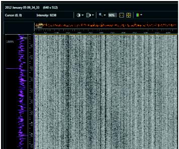
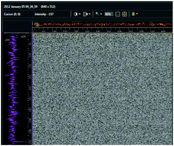
Fixed Pattern Noise is a form of background non-uniformity where structured patterns are visible in the ‘bias’ image of a camera.
Typically, this pattern noise will manifest in the form of column variations. In a typical InGaAs FPA camera, each column is connected to an individual preamplifier for readout. These preamplifiers will likely exhibit some variation in the offset (the value the camera outputs at zero incident signal), and gain (the ratio of detected photoelectrons to displayed grey levels). Without correction, these variations can carry through into the image in the form of static vertical stripes.
The correction applied takes two forms: Firstly, the offset variation can be removed through background subtraction – an essential step in practically all InGaAs imaging. The images to the right demonstrate the ‘before’ and ‘after’ of this process using Teledyne Princeton Instruments LightField data acquisition software.
The second form is the removal of gain variations is through careful calibration of the sensor response. This is performed in-house by Teledyne Princeton Instruments engineers before the camera is shipped.
Pixel Defects
InGaAs cameras typically show a small number of individual pixels that have a dark current response much higher or much lower than the mean. These are called pixel defects, and can be present as just a single pixel, or sometimes 2 or 3 neighboring pixels.
These are corrected through a nearest neighbor correction, inferring the likely value of the pixel from surrounding pixel values, restoring image quality.
The pixel defects present on a camera are mapped by Teledyne Princeton Instruments engineers before the camera is shipped, and these can be easily corrected within the Teledyne Princeton Instruments LightField software. The list of pixel defects can be seen and edited in case the user would like to add additional points.
Charge Traps & Star Defects
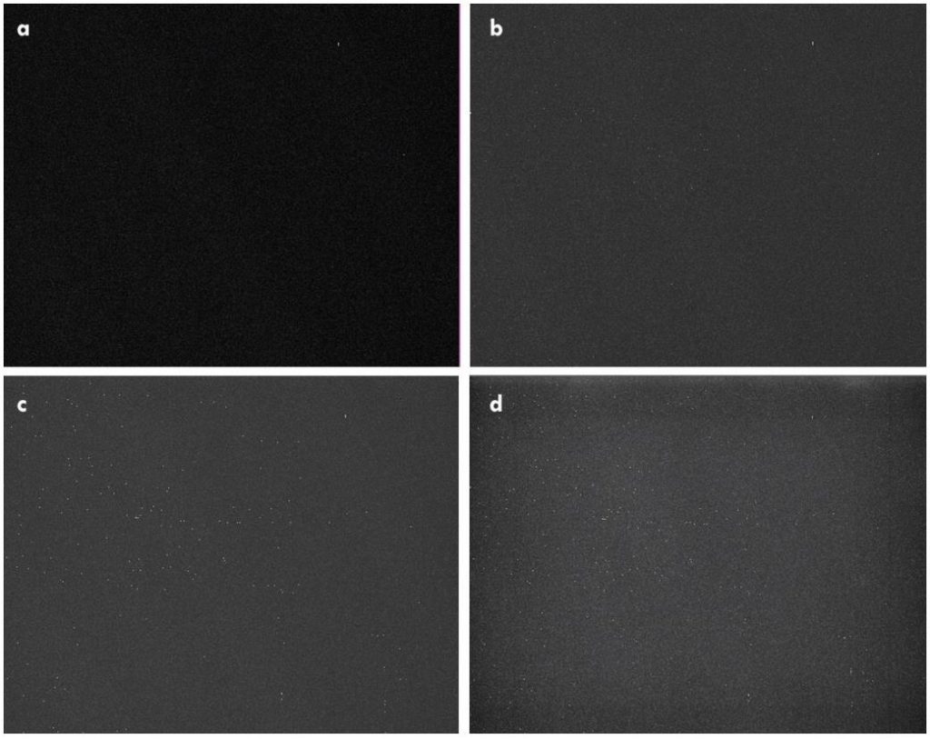
Star defects are an InGaAs-specific defect in the form of a ‘star’ shape. These can take two forms: Bright center star defects occur when a so-called ‘charge trap’ in the central pixel either steals photoelectrons from neighboring pixels, leaving them darker than the true response. Dark center star defects occur when the charge trap distributes its collected charges to its neighbors, resulting in a dark pixel surrounded by brighter pixels. A bright center star defect is shown to the right.
At Teledyne Princeton Instruments, we have a proprietary algorithm to find and correct star defects, resulting in far cleaner, more quantitative data.

Blemishes & Clusters
Occasionally many defects can bunch together into what’s called a cluster or a blemish. In this case, anything up to around 15 pixels across a small area can show anomalous high or low signals as in the case of the ‘Pixel Defect’ above, but in this case, a naïve ‘nearest neighbor’ correction would not be appropriate, as the neighbors may include other defective pixels.
As a result, the location of clusters or blemishes on the sensor of the NIRvana camera range is also mapped by our engineers, and included in the defect map that LightField uses for correction. This allows a more accurate correction to be performed.
Summary
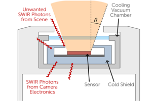
The defects present on InGaAs cameras, if uncorrected, present a major barrier to image quality and analysis. Through our expertise in scientific imaging, the NIRvana camera range, from Teledyne Princeton Instruments, can provide a significantly more accurate and comprehensive correction of defects and artifacts. Along with our world-leading thermal management and low noise giving superior signal-to-noise ratio at any exposure time, integrated cold shielding to protect the sensor from unwanted external infrared photons and powerful software, the NIRvana range of cameras is the perfect fit for demanding scientific applications in SWIR.
Further Reading
How NIRvana Cameras Keep Their Cool
Find out about the industry-leading thermal management performance of the NIRvana InGaAs camera range
Cold Shielding in SWIR
Find out about the advantages of Cold Shielding, and how the NIRvana range utilizes it to minimize background SWIR signal.
The Powerful Sensitivity of NIRvana Cameras
Find out more about how the NIRvana range improves signal-to-noise-ratio and provides powerful sensitivity.