
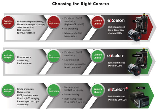
Introduction
Since their invention in 1969, charge-coupled devices (CCDs) have been used to detect the faint light from items as nearby as cells under a microscope to those as far away as stellar objects at the edge of the known universe. Over the past four decades, low-light CCD cameras have facilitated some of the biggest breakthroughs in both the life sciences and the physical sciences. Salient features that have contributed to the remarkable track record of these detectors include greater than 90% peak quantum efficiency (QE), very low read noise of 2 e- rms or less, 100% fill factor, and excellent charge-transfer efficiency.
About twelve years ago, a variant of CCDs known as electron-multiplying CCDs (EMCCDs) were developed. In addition to the features noted above, EMCCDs are able to achieve sub-electron read noise at high frame rates, allowing single-photon detection. Thus, CCD and EMCCD cameras are commonly the instruments of choice for scientific applications ranging from steady-state astronomical imaging to dynamic single-molecule imaging, and from widefield imaging to spectroscopy.
This paper provides a basic overview of the advantages and disadvantages of various types of low-light CCDs and introduces an advanced sensor technology, eXcelon, that mitigates some of their inherent limitations.
Types of CCDs
Scientific-grade CCDs afford researchers a number of distinct technologies from which to choose. Primary CCD types include front-illuminated CCDs, standard thinned back-illuminated CCDs, and standard back-illuminated deep-depletion CCDs.
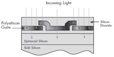
In a traditional front-illuminated CCD, light passes through the polysilicon gates that define a charge well at each pixel (see Figure 1). While the gates transmit a number of the incident photons to the CCD’s photoconversion layer, they also reflect and absorb a fraction of photons, thereby preventing some light from reaching the pixel’s photosensitive region. As a result, front-illuminated devices typically offer only about 50% QE (i.e., the fraction of incident photons contributing to the signal).
To improve QE, devices can be uniformly thinned via acid-etching techniques to attain approximately 10 to 15 μm thickness so that an image can be focused directly onto the photosensitive area of the CCD (i.e., the depletion region), where there is no gate structure. Compared to front-illuminated CCDs, these thinned back-illuminated devices have a higher QE (>90%) across the visible spectrum.
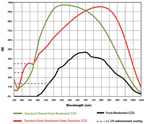
To further improve QE, especially for near-infrared (NIR) imaging and x-ray applications, a bias voltage can be applied to a layer of high-resistivity silicon ranging from 50 to 300 μm thickness in order to produce a “deeper” depletion region (i.e., active photosensitive area). This architecture allows longer-wavelength photons to interact within the layer as opposed to merely penetrating it, ultimately helping to increase QE (see Figure 2).
Advantages and disadvantages
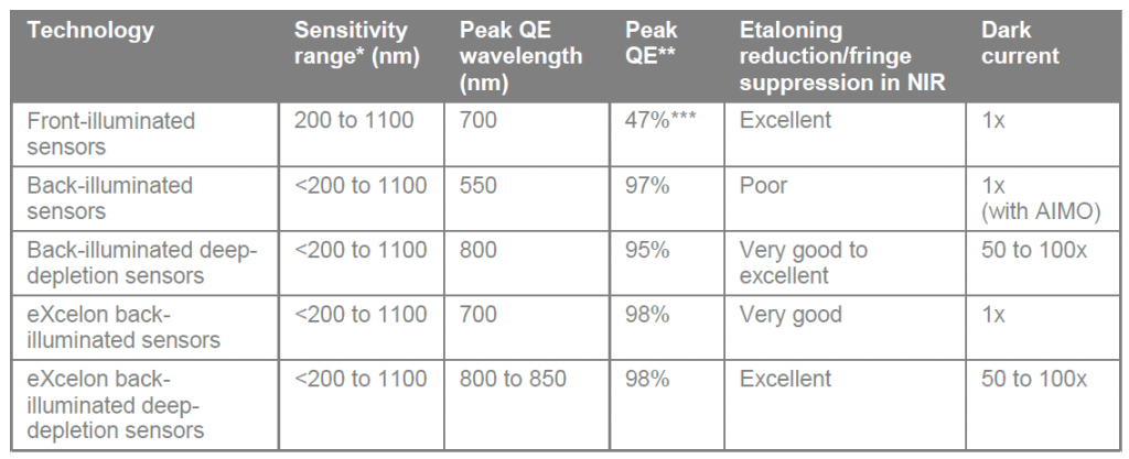
Table 1 briefly summarizes the main advantages and disadvantages of the aforementioned technologies in relation to low-light imaging and spectroscopy applications. Overall, front-illuminated CCDs are relatively inexpensive, but provide lower sensitivity (refer to Figure 2). In the NIR, they have 2x to 3x lower QE than back-illuminated CCDs. It is worth noting, however, that front-illuminated CCDs may be preferable for certain high-light-level NIR applications, as they do not suffer from etaloning.
In addition to the deep-depletion technology on the market today, there have been several designs calling for fully depleted sensors featuring silicon that is 100 to 300 μm thick. Such devices promise to provide further improvement in NIR sensitivity, but have yet to be made available on a large commercial scale.
eXcelon technology for CCDs
Until recently, researchers whose applications require low-light broadband photon detection had to choose between cameras that utilize either standard thinned back-illuminated or standard back-illuminated deep-depletion technologies. Although both of these options are capable of delivering extremely high sensitivity, their performance is nonetheless compromised to a certain extent by the limitations described in the preceding section. Recently, Teledyne Princeton Instruments developed sensors (and associated cameras) that minimize and even eliminate some of these hindrances.
While the precise details regarding the novel technology are beyond the scope of this primer and cannot be revealed for intellectual property reasons, the benefits of eXcelon can be explained via comparative measurements.
Novel eXcelon sensors are based on a standard back-illuminated architecture and provide three significant advantages over the other technologies under discussion:
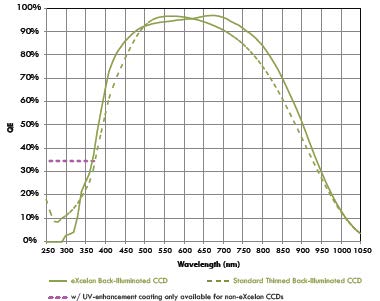
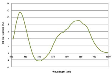
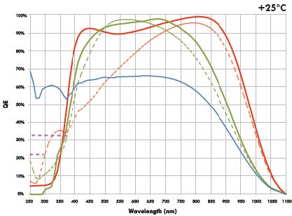
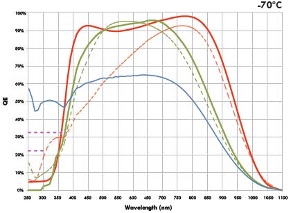
First, consider the sensitivity of eXcelon technology. Figure 3 shows that eXcelon back-illuminated CCDs provide higher sensitivity below 500 nm and above 625 nm than standard thinned back-illuminated sensors. The small (2 to 3%) drop in the green region can generally be tolerated, especially taking into account the other benefits that this technology offers. The relative gain in QE using eXcelon technology is plotted in Figure 4, which estimates a 15 to 20% maximum increase.
**Typical data at +25°C ***Virtual-phase front-illuminated sensors may provide higher QE (albeit still far lower than back-illuminated sensors)Figure 3. The typical front-illuminated sCMOS sensor architecture (left) relies on the use of microlenses. Back-illuminated sCMOS sensors (right) do not utilize microlenses.
Table 1. Main advantages and disadvantages of various sensor technologies.
Novel eXcelon sensors are based on a standard back-illuminated architecture and provide three significant advantages over other advanced technologies
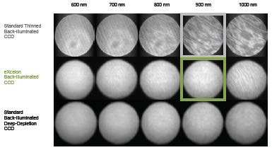
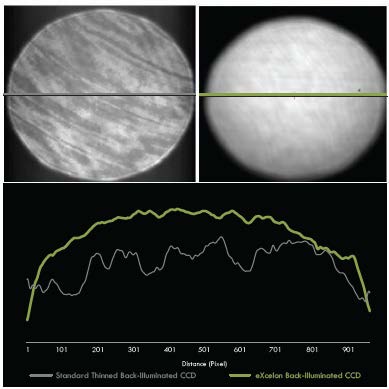
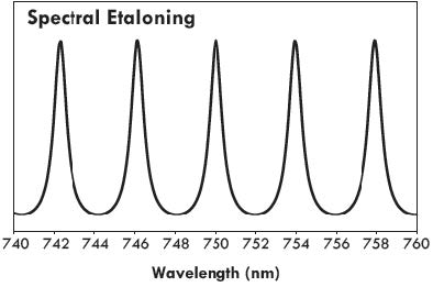
Another key eXcelon advantage is the novel technology’s lower etaloning in the NIR. Figure 5 presents a series of images showing the etaloning performance of cameras utilizing standard thinned back-illuminated CCDs, eXcelon back-illuminated CCDs, and standard back-illuminated deep-depletion CCDs. Figure 6 also shows that eXcelon-enabled cameras offer far less etaloning than cameras configured with a standard thinned back-illuminated sensor.
Finally, since original eXcelon technology is based on a standard thinned back-illuminated architecture, it has similar dark current (i.e., 100x lower than that of standard back-illuminated deep-depletion CCDs). In other words, standard back-illuminated deep-depletion CCDs require deeper cooling to achieve similar dark noise performance as that of eXcelon detectors. This is an important consideration, especially in spectroscopy, where signal is integrated over many minutes and binned over several rows.
eXcelon back-illuminated deep-depletion CCD technology
Teledyne Princeton Instruments has also added eXcelon technology to back-illuminated deep-depletion CCDs in order to further improve sensitivity and etaloning performance compared to standard back-illuminated deep-depletion CCDs.
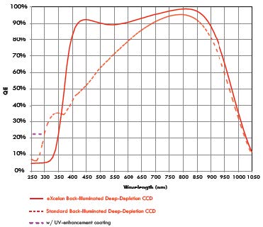
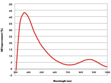
Figures 7 and 8 show the improvement in QE that can be achieved with eXcelon-enabled back-illuminated deep-depletion CCD technology. The broader wavelength coverage of these sensors in the NIR (>800 nm) and blue regions (>350 nm) is noteworthy. This is particularly appealing for applications such as cold atom/ion imaging in which researchers are interested in either the NIR or blue region, depending on the atoms/ions used.
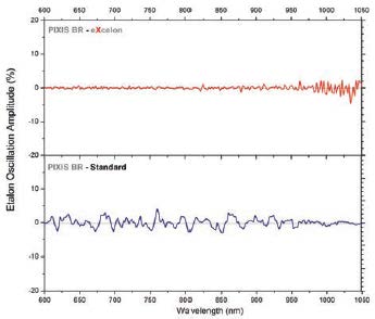
These eXcelon back-illuminated deep-depletion sensors also provide the lowest etaloning available, even lower than the performance offered by standard back-illuminated deep-depletion sensors. The measurements presented in Figure 9 show this etalon oscillation reduction.
Ways to further improve sensitivity
While sensor technology is an important determiner of camera system sensitivity and signal-to-noise ratio in a given experiment, factors such as optical window throughput are also important.
To maximize light throughput, Teledyne Princeton Instruments uses a highly advanced single-window vacuum design (see Figure 10). This means the vacuum window is the only optical surface encountered by incident photons before they reach the CCD detection surface. Although the design is the best available, each uncoated optical surface of the vacuum window can still have 3 to 4% transmission loss, or a total loss of 6 to 8%.
For light-starved imaging applications, this loss can result in a significant reduction of signal-to noise ratio. Moreover, any light reflected inside the system can lead to glare and fringing, especially when used with coherent illumination. The solution is to apply anti-reflective (AR) coatings on the window in the optical path, which reduces total losses to below 1% and sometimes even to less than 0.5%. For applications utilizing extremely coherent light sources, a wedge window may also be required to eliminate glare and fringing.
Teledyne Princeton Instruments cameras are designed with a single window made of high-grade fused silica/quartz/MgF2 that acts as a vacuum viewport. Any shipping-protection windows on the CCD are removed prior to installing it in the vacuum chamber. The vacuum window, which is brazed (a high-temperature fusion process at the molecular level) to the vacuum chamber, can be customized with single- or multiple-layer AR coatings to match the wavelength of interest (see Figure 11). It should be noted that AR coatings typically provide the best performance when they are tuned for a narrow wavelength range. Since they may have poorer transmission outside their optimum wavelength range, care must be taken before choosing an AR coating.

Conclusions
Developed by Teledyne Princeton Instruments, eXcelon back-illuminated sensor technology provides higher sensitivity (over a broad wavelength range) as well as lower etaloning than standard back-illuminated sensor technology. For most applications in which standard thinned back-illuminated sensors are commonly utilized, eXcelon now offers researchers superior performance (see Figure 12).
For applications that require extremely high sensitivity and the lowest etaloning in the NIR, eXcelon back-illuminated deep-depletion sensors are the best choice. However, to keep dark noise at a minimum, these detectors must be cooled. For spectroscopy applications such as Raman, either deep thermoelectric cooling or liquid nitrogen cooling is recommended.
Front-illuminated sensors, meanwhile, remain a highly cost-effective option, as long as substantially lower QE is acceptable to the user.
Appendix A: Etaloning in the NIR
Standard thinned back-illuminated CCDs are solid-state imaging devices that have been etched to 10 to 15 μm thickness in order to collect light through the back surface. As a result of this modification, no light is lost via absorption and reflection by the polysilicon gate structure; these CCDs have more than twice the QE of their front-illuminated counterparts. An unfortunate side effect of this process is that the devices become semi-transparent in the NIR. Reflections between the parallel front and back surfaces of these CCDs cause them to act as partial etalons. This etalon-like behavior leads to unwanted fringes of constructive and destructive interference, which artificially modulate a spectrum. The extent of modulation can be significant (more than 20%) and the spectral spacing of fringes (typically 5 nm) is close enough to make them troublesome for almost all NIR spectroscopy.
An etalon is a thin, flat transparent optical element with two highly reflective surfaces that form a resonant optical cavity. Only wavelengths that fit an exact integer number of times between the surfaces can be sustained in this cavity. Because of this property, etalons can be used as comb filters, passing just a series of uniformly spaced wavelengths. In an imperfect etalon, the reflectance of the surfaces becomes less than 100% and the spectral characteristics soften from a spiky comb to a smooth set of fringes. Absorption between the surfaces also worsens the quality of the resonant cavity, which is measured by cavity finesse (see Figures A-1, A-2, and A-3).
Thus, the three factors that determine the shape and character of an etalon are d, the distance between the two surfaces; λ, the wavelength of the light; and Q, the finesse of the cavity, as shown in the following equation (where I is intensity):


At NIR wavelengths, the silicon of which CCDs are made becomes increasingly transparent, causing the QE to decline in the red. The back surface, where light enters a CCD in the back-illuminated configuration, is typically AR coated. These coatings are not perfect, however, and their effectiveness varies by wavelength. Most CCD back-surface AR coatings are not optimized for the NIR.
For example, the reflection from the back surface of a CCD that is optimized for ultraviolet (UV) response is worse in the NIR than that from a CCD whose AR coating is optimized for longer wavelengths.
Once light has passed through the body of a CCD and is about to reach the polysilicon electrodes, it encounters a sandwich of layers that generally includes silicon dioxide (refractive index 1.5). This sizeable discontinuity from the refractive index of silicon (which is 4) produces a large reflection back into the CCD. At wavelengths where silicon is transparent enough that light can traverse the thickness of the CCD several times, light bounces back and forth between the two surfaces. This increases the effective path length in the silicon (enhancing the QE) and also sets up a standing wave pattern. Amplitude is lost at both reflective surfaces and by absorption in the body of the silicon. However, at longer wavelengths, sufficient amplitude survives to cause significant constructive or destructive interference.
While silicon is usually thought of as opaque, it must be remembered that a standard back-illuminated CCD is typically only 10 to 15 μm thick (less than a thousandth of an inch). A layer this thin can transmit a significant fraction of NIR light. For example, a back-illuminated CCD that is 15 μm thick (mechanically) would have the effective optical thickness of about 60 μm (since the refractive index of silicon in this wavelength range is 4). Thus, the round-trip optical path length between the surfaces is approximately 120 μm. At 750 nm, this would be 160 wavelengths. Therefore, there would be constructive interference at 750 nm. This pattern of interference would continue to repeat with intervals of about 5 nm.
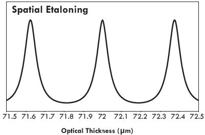
In addition to the spectral source of etaloning, in a thinned CCD there can also be spatial etaloning. The spatial pattern arises from the incidence of monochromatic light on an etalon whose thickness is not perfectly constant. A small variation in thickness can change the local properties from constructive to destructive interference. The change required is only a half-wavelength in the roundtrip path length. Since the index of silicon is 4, the change in CCD mechanical thickness required to produce this optical effect is only about 1/16 of a wavelength, or 0.05 μm at a wavelength of 800 nm. This effect can actually be used to visualize how uniform the thickness of a CCD is. If a CCD had perfectly uniform thickness, the modulation due to spatial etaloning at a given wavelength would disappear. All pixels would have the same degree of constructive or destructive interference at a given wavelength.
In most imaging applications with standard thinned back-illuminated CCDs, spatial etaloning is not evident because the applications are at shorter wavelengths, where the silicon absorption damps out the etalon effect. In addition, many applications use light that is spectrally broad enough to span (and average out) several etalon-fringe cycles. The latter requires only a spectral bandwidth of a few nanometers. In a spectrometer, by comparison, the light on any one column of pixels is very narrow spectrally, typically less than 0.1 nm. Thus, this spectral bandwidth is much less than the period of etalon cycles (~5 nm). As a result, spatial etaloning is quite evident when viewing an image of a uniform spectrum (e.g., tungsten bulb) in the NIR (see Figure A-4).

Spectroscopic etaloning is related to, but different from, spatial etaloning. It derives from the fact that in a spectrometer the wavelength of light varies across the CCD. Thus, even if a back-illuminated CCD was available with absolutely uniform thickness, it would still show fringes due to this etalon effect. The fringes in this case are due to the variation of the wavelength, not the thickness. As a result, when a spectrum is dispersed across a back-illuminated CCD, the characteristic comb pattern will be superimposed on the normal response.
Appendix B: Effect of cooling on QE
In addition to the sensor technology type and factors such as optical window throughput, cooling the detector has an effect on QE. Typically, cooling decreases long-wavelength coverage due to a change in electron mobility and effective path lengths. Figure B-1 presents a theoretical estimate of QE as various sensors are cooled.

Application CTA Section
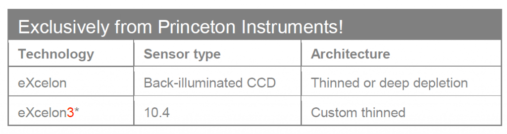
eXcelon 3® Technology for EMCCD
Primer discussing the advantages of eXcelon3 for EMCCD technology.

Get In Touch
Speak to a member of our team about your specific application, and what we can do to help you.

Join Our Mailing List
Make sure that you aren’t missing out on anything by joining our mailing list