
Introduction
CCDs have become increasingly specialized to meet the changing requirements of both commercial and scientific markets. In the scientific market, CCDs have been improved and optimized in a variety of ways to provide high performance across a broad set of applications — from spectroscopy and semiconductor testing to biological imaging and genetic research.
Design modifications to scientific-grade CCDs, initially driven by interest in x-ray astronomy applications, have greatly expanded the domain of x-ray imaging and x-ray spectroscopy at synchrotron facilities. Devices have been engineered to detect x-rays in the energy range extending from well below 100 eV all the way up to 100 keV and higher (a full three orders of magnitude), making them invaluable for research in which high sensitivity is combined with two-dimensional detectors. These devices are utilized in many x-ray techniques, including x-ray microscopy, x-ray lithography, x-ray spectroscopy, x-ray crystallography, and x-ray non-destructive testing.
In direct-detection cameras, the CCD is directly exposed to the incoming x-ray photons, which enables direct absorption (i.e., detection) of the photons. Depending on the x-ray energy range, either a back-illuminated CCD without anti-reflection (AR) coating, or a front- or back-illuminated, deep-depletion CCD is used.
Basic Principles
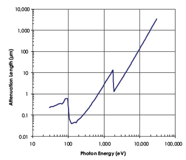
When exposed to visible light (380-750 nm), front- and back-illuminated CCDs generate a single electron-hole pair in the epitaxial layer for each absorbed photon. The optimal layer thickness required to achieve the highest quantum efficiency (QE) in these devices varies with wavelength. Manufacturers of front- and back-illuminated CCDs have settled on thicknesses of ~20 μm and 15 μm, respectively. Although these standard thicknesses can absorb x-rays in the range from approximately 30 eV to 20 keV (Figure 1), other components within the CCD help dictate the type of device needed to detect low- and medium-energy x-rays.
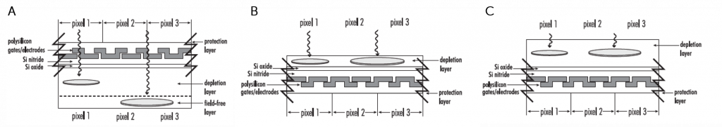
For instance, because both the electrode structure and the insulating layer of a front-illuminated CCD will absorb x-ray photons below energies of 700 eV, a back-illuminated CCD architecture is required to detect low-energy x-rays (about 30 eV to 3 keV). The cross section of a back-illuminated CCD is shown in Figure 2.
When it comes to low energy x-rays (approximately 30 eV to 500 eV) even AR coating itself can absorb x-ray photons. With this in mind, Teledyne Princeton Instruments designed its direct-detection cameras without AR coating. For medium-energy x-rays (about 3 keV to 20 keV), back-illuminated CCDs with or without AR coating can be used.
To meet the demand for higher QE in the medium energy x-ray range, CCD manufacturer Teledyne e2v developed front-illuminated, deep-depletion technology several years ago as a way to increase sensitivity. To achieve a favorable balance between QE, spatial resolution, and blemishes, Teledyne e2v utilizes a 50 μm-thick epitaxial layer. To optimize detector QE, Teledyne Princeton Instruments PIXIS-XB utilizes these sensors in conjunction with a beryllium window, a design that gives researchers the freedom to use the camera without having to attach the detector to the vacuum chamber.
For extremely demanding applications that require x-ray sensitivity spanning the low-to-medium energy range (about 30 eV to 20 keV), Teledyne Princeton Instruments has also designed the SOPHIA-XO and PIXIS-XO cameras that uses a back-illuminated, deep-depletion CCD without AR coating. These models feature a rotatable ConFlat flange, but alternatively it can be supplied with a removable ConFlat flange with a beryllium window. Finally, for ultimate operational flexibility within the vacuum chamber, Teledyne Princeton Instruments offers the PI-MTE3 camera, which can be delivered with any of the aforementioned CCD sensors.
Charge-Generation Mechanism
X-ray photons traveling through the layers of a CCD can lose energy through Compton scattering, fluorescence, or the photoelectric effect. For energies less than 150 keV, the photoelectric effect is dominant. Thus, when an x-ray photon in the 30 eV to 20 keV energy range is absorbed in the silicon, its energy is converted via the photoelectric effect and generates electron-hole pairs in the CCD based on the primary x-ray photon energy. To produce one electron-hole pair in silicon, an x-ray photon requires an average of 3.65 eV per pair. Therefore, when an x-ray photon of 8.0 keV is absorbed it generates about 2192 e- (8000/3.65). Note that fluctuations in the average energy required to produce an electron-hole pair are governed by the interaction of x-ray photons within the silicon. These fluctuations are summarized by a numerical factor called the Fano factor (0.1 for silicon).
Charge-Collection Mechanism
For scientific applications that place a high premium on quantitative measurements, it is important that the charge generated by an x-ray photon is collected within one pixel and then transported to the output amplifier without suffering losses from imperfect charge-transfer efficiency (CTE). Depending on its generation locale, there is some probability that the photoelectron charge cloud will be split between two or more pixels. This level of uncertainty must be accounted for in order to ensure the most accurate data.
If the charge is generated in a field-free layer, then it moves by diffusion and either recombines or reaches the edge of the depletion layer field. Any charge that reaches (or is generated within) the depletion layer is swiftly drifted to the surface collection site with minimal radial spread. Charge that is generated close to the edge of a pixel, or deep in the substrate, can split between pixels. Some charge from deeply generated events may also recombine so that the charge is not conserved.
The measurement of signal charge does not always indicate the true deposited energy, particularly for events generated deep in the CCD (high-energy x-rays in the case of a front-illuminated device). Some partial events may also be evident in a pulse height distribution generated from a monochromatic x-ray source.
In a back-illuminated device, in which the field-free layer is etched out, the electrons are generated directly in the epitaxial layer. Therefore, in this case, migration of generated electrons can also occur in lower-energy x-rays, as they are generated near the surface.
When the detector is used in a photon-counting mode, steps should be taken to ensure that (1) the incoming flux, related to the exposure time, is weak enough to prevent multiplex-ray photons from reaching the same pixel and (2) a method to differentiate single-pixel events from multiple-pixel events has been implemented in the system (Figure 3). Typically, an intensity-threshold method is used to distinguish between single-pixel and multiple-pixel events. To utilize this method, precise threshold levels for single-pixel events and multiple-pixel events must be selected, as illustrated in the following example.
Radiation Damage
The good sensitivity and higher QE attained with CCDs designed for direct x-ray detection comes with an inherent trade off, namely once a significant quantity (i.e., dose/flux) of x-ray radiation has bombarded the CCD, permanent damage occurs. In particular, the following changes in performance parameters are observed:
Increase in dark current: As x-ray photons strike the silicon they create additional interface states between the silicon and the silicon-dioxide gate oxide. These new states have energy levels within the silicon band gap and lead to an increase in dark current.
Flat-band voltage shift: When x-rays are absorbed in the gate oxide, electron-hole pairs are generated. Some of the electrons are detected as signal, some of them recombine, and the remaining electrons escape from the oxide. The mobility of the holes, however, is much lower than that of the electrons; thus, some holes become trapped in the oxide. These trapped holes result in a positive space-charge build up that modifies the gate potential and increases the potential in the active region of the epitaxial silicon. The effect is referred to as a flat-band voltage shift. If the charge build up becomes too large, the CCD clock and bias voltages may have to be adjusted to maintain device performance.
Reduction in CTE: If the energy of the radiation is high enough, displacement damage will occur in the silicon lattice. In turn, CTE will be diminished. To displace silicon atoms, electron kinetic energy of approximately 150 keV is required. In back-illuminated CCDs, incident photons reach the epitaxial layer before encountering the gate structure. Therefore, radiation damage does not occur at energy levels that fall below a device-specific threshold within the low-energy x-ray range. Even at energy levels where x-rays reach the electrode structure, radiation damage is delayed.
These parameters are affected differently by various types of radiation — namely protons, neutrons, and heavy ions (energetic particles), as well as electrons, gamma rays, beta rays, and x-rays (ionizing radiation). Performance degrades slowly as the dose of ionizing radiation builds up, but very rarely reaches the catastrophic levels that can result in sudden failure. Therefore, the specific radiation dose that marks the end of useful life can vary widely depending on the application, the x-ray energy, and the radiation flux. Some of these effects are intrinsic to all silicon-based devices, but others are related to CCD structures and manufacturing processes.
Annealing Damage
It has been reported that if a device with high dark current due to x-ray irradiation is treated in forming gas (10% H2 90% N2) at about 350 °C for a few hours, the CCD’s performance can be restored to its pre-irradiation level.
It has also been reported that if exposed to a 254 nm UV wavelength source (EPROM-erasure light source) for about 10 minutes, the shift in various voltages can be reduced.
Note that these treatments may render the CCD more susceptible to future x-ray damage. However, if the device is annealed at 100 °C for about 15 hours in air after the completion of the 350 °C forming gas annealing, then this effect may be countermanded.
None of the experiments listed in this section has been performed in Teledyne Princeton Instruments’ lab, therefore we strongly recommend that caution be exercised when attempting these procedures. Depending on the amount of damage to a specific CCD, either the temperature or the hours of exposure may have to be adjusted.
Further Information
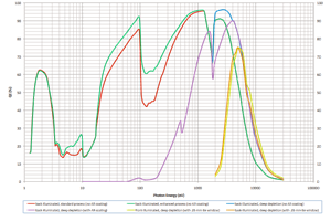
QE Response Curves for the Soft X-Ray – VUV
Technical note describing how sensor design effects quantum efficiency for soft x-ray and VUV applications.
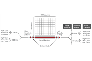
Flexible Electronic Architecture Extends Camera Utility
Technical note describing how flexible electronic architecture can be advantageous for multiple applications within x-ray research.
Utilizing Phosphors for Indirect Detection of X-rays
Technical note describing the two types of phosphors used for x-ray imaging applications between the energy ranges 5 keV and 50 keV.