
A Quantitative Comparison of Different Scientific CCD Types
Overview
Since the invention of charge-coupled-device (CCD) technology in 1969, its extended sensitivity from the NIR to the x-ray region of the electromagnetic spectrum has been utilized to good effect in a wide variety of application areas (e.g., astronomy, Bose-Einstein condensates, fluorescence imaging, photometry, plasma research, Raman spectroscopy, and x-ray imaging).
Owing to the unique characteristics of their construction, CCDs are especially useful for imaging and spectroscopy performed in the soft x-ray to VUV range. However, due to the strong absorption of UV radiation by materials utilized in the layer above the CCD’s epitaxial photon-absorption layer (depletion layer), it is very important to make sure that any layer above the depletion layer is as thin as practically possible.
As advanced applications like EUV lithography (a next-generation semiconductor manufacturing process) continue to gain traction in science and industry, the demand for imaging tools that are extremely stable and sensitive in the soft x-ray to VUV energy range is increasing. To address the challenge, special enhanced-process and other back-illuminated CCDs without AR coating now provide unprecedented sensitivity in the soft x-ray to VUV range.
This document presents the quantum efficiency for several types of CCDs: (1) standard-process, back-illuminated CCDs; (2) enhanced-process, back-illuminated CCDs; (3) deep-depletion, back-illuminated CCDs; and (4) deep-depletion, front-illuminated CCDs. Sensitivity differences within the soft x-ray to VUV energy range are evident.
Comparison: Cross-Sections & Depletion Depths
The schematic cross-sections of two back-illuminated CCD types, one that utilizes a regular-depth depletion layer and one that features a deep depletion layer, are shown in Figure 1. Each drawing illustrates the differences between the depletion region and the field-free region in the silicon. Electrons generated in the depleted region are captured in the pixel in which they are generated. Electrons generated in the field-free region will diffuse until they enter a depletion region, at which point they will be captured in the pixel under it. It should also be noted that, in general, anti-reflective coatings adversely affect a CCD’s ability to detect soft x-rays.
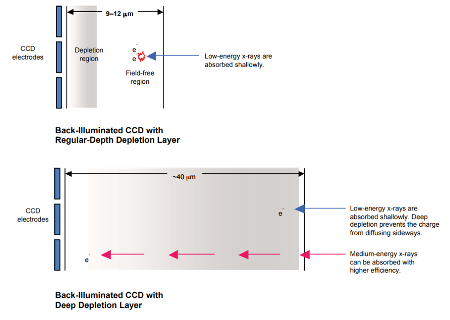
Table 1 shows the typical overall silicon thickness, the thickness of the field-free region, and the thickness of the depleted region for various back-illuminated CCD types. Notice the enhanced-process device, which delivers the highest CCD sensitivity to date for the 100 eV to 250 eV energy range.
| CCD Type | Overall Thickness (µm) | Field-Free Layer (µm) | Depleted Layer (µm) |
| Regular-depth depletion (standard process) without AR coating | 12 | 6 | 6 |
| Regular-depth depletion (enhanced process) without AR coating | 9 | 3 | 6 |
| Deep-depletion device with or without AR coating | 40 | 2 | 38 |
Figure 2 is a schematic cross-section of a front-illuminated, deep-depletion CCD. Note that the x-rays enter the CCD through the gate electrodes. Low-energy photons are absorbed in the gate structure and do not reach the sensitive silicon.
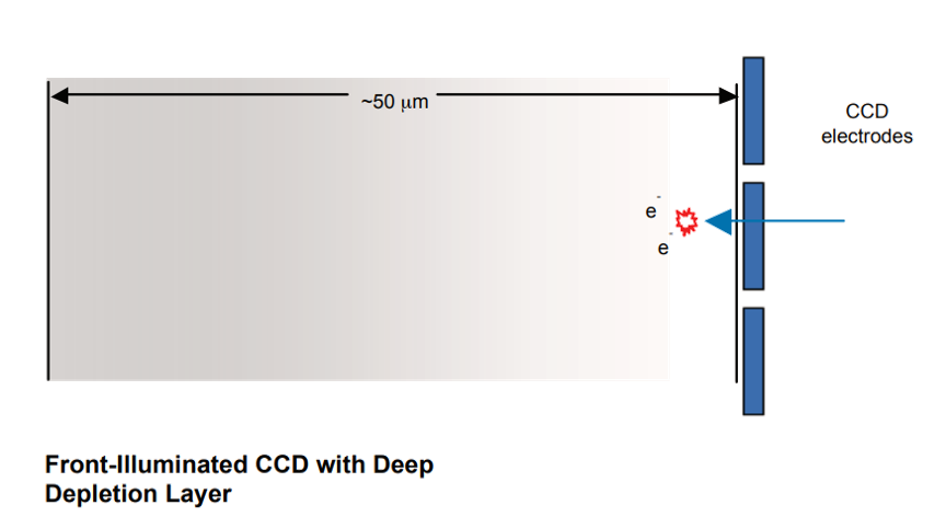
Table 2 shows the typical overall silicon thickness, the thickness of the field-free region, and the thickness of the depleted region for a front-illuminated, deep-depletion CCD. Note that the device can be utilized with a beryllium window to improve soft x-ray transmission. (Beryllium windows can also be used with back-illuminated CCDs.)
| CCD Type | Overall Thickness (µm) | Field-Free Layer (µm) | Depleted Layer (µm) |
| Deep-depletion device with or without Be window | 50 | 12 | 38 |
Comparison: Quantum Efficiency
Figure 3 presents the QE response for different types of scientific CCDs in the energy range from 0.1 eV to 30 keV. In particular, note the higher quantum efficiency between 100 eV and 250 eV provided by the enhanced-process, back-illuminated CCD.
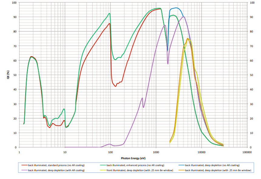
The data above is critical for selecting the right CCD type to meet an application’s sensitivity requirements.
Additional Reading
- S. Hubert and V. Prévot, “Quantum efficiency measurements of an x-ray charge-coupled device in the 2–10 keV spectral region by means of a double crystal monochromator coupled to an x-ray tube,” Appl. Opt. 53(34) 8078–8085 (2014).
- P. Boerner et al., “Initial calibration of the atmospheric imaging assembly (AIA) on the solar dynamics observatory (SDO),” Solar Phys. 275(1) 41–66 (2012).
- R.A. Stern et al., “Characterization of the flight CCD detectors for the GOES N and O solar x-ray imagers,” Proc. of SPIE 5171 77–88 (2004).
- J.-P. Wülser et al., “EUVI: the STEREO-SECCHI extreme ultraviolet imager,” Proc. of SPIE 5171 111–122 (2004).
- L. Poletto, A. Boscolo, and G. Tondello, “Characterization of a charge-coupled-device detector in the 1100–0.14-nm (1-eV to 9-keV) spectral region,” Appl. Opt. 38(1) 29–36 (1999).
Further Information

HHG and High-Sensitivity Cameras for Soft X-ray Applications
Find out the work from researchers in the Attoscience and Ultrafast Optics ground at the Institute of Photonic Sciences on HHG for NEXAFS spectroscopy.
Flexible Electronic Architecture Extends Camera Utility
Technical note describing how flexible electronic architecture can be advantageous for multiple applications within x-ray research.
Direct Detection of X-rays using CCD Technology
The fundamentals of CCD technology and how it is optimized for the direct detection of x-rays.