
Introduction
CMOS sensor technology has steadily improved over the last decade, and is now the standard for many applications such as security, machine vision, and handheld imaging systems. Compared to long established sensor technologies such as CCD and EMCCD, CMOS delivers the optimal combination of speed, noise performance, low power and compact size. In addition, large scale production of these sensors has enabled the expansion of vision technology into many new and expanding markets.
However, two factors have limited the adoption of CMOS sensors into more demanding applications. Firstly the ‘rolling shutter’ architecture of CMOS devices can introduce artifacts for imaging dynamic objects, not present with the ‘global shutter’ architecture of CCD and EMCCD sensors. Secondly the reduced quantum efficiency (sensitivity to photons) of so-called ‘front-illuminated’ CMOS, compared to the more sensitive ‘back-illuminated’ sensors common for CCD and EMCCD.
Scientific CMOS sensors have been developed previously able to improve on one of these factors, but never both. But thanks to innovations in the design of LACera™ Technology sensors, global shutter, back-illuminated sensors are now possible in scientific imaging, enabling CMOS technology to lead the way in yet more imaging applications.
What is Global Shutter?
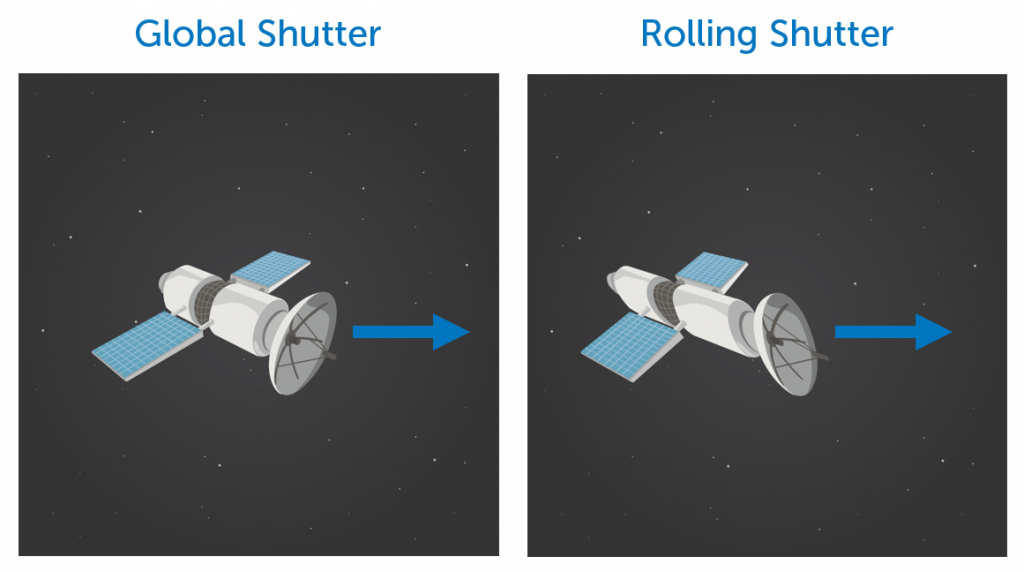
When cameras have finished exposing an image, the acquired signal must be read out. The pixel will be reset, the signal in the form of collected photoelectrons cleared, and the sensor made ready to expose the next frame. Ideally, this process should happen simultaneously across the entire sensor as found in full frame CCD’s. For the majority of CMOS cameras however, this process is performed row-by-row, ‘rolling’ down the sensor, called a rolling shutter. This means the exposure of the sensor to light occurs at different times for each line of l the sensor. This is shown in Figure 1A below.
In applications where there is no relative motion between the subject and the camera, rolling shutter is not an issue. However, in dynamic scenes, due to motion or varying light/signal intensity, rolling shutter mode will introduce image distortions. These ‘rolling shutter artifacts’ are discussed more on the next page. For many imaging applications, a far more desirable sensor modality would be a Global Shutter which exposes and resets every row of the camera simultaneously, as shown in Figure 1B.

Limitations of current CMOS cameras
Rolling Shutter Artifacts
When imaging moving objects, or moving a camera’s field of view during acquisition, all cameras are susceptible to some imaging artifacts such as motion blur when using an exposure time that is long compared to the motion of the object. But for rolling shutter cameras, an additional artifact can be introduced if any movement is of a similar timescale to the rolling shutter sequence.
For large-scale movements such as large objects in view, or simultaneous movement across the whole field of view, the ‘frame time’, which is the time between the start of the exposure of the top and bottom lines as shown in Figure 1, is the relevant timescale. For CMOS cameras, frame times vary but can typically be around 20ms. If the object moves visibly during 20ms, rolling shutter artifacts such as Figure 2 will be visible.
For small-scale movements, for example an object that covers only several pixels of the field of view, faster movements can still be captured, as now the ‘line time’, the time for the rolling shutter to move from one line to the next, is relevant. This is the frame time divided by the number of rows, typically around 10 microseconds.
With global shutter acquisition, these artifacts are avoided, which can be key for many applications. Global shutter CMOS cameras are more rare than rolling shutter CMOS cameras, and producing highly sensitive global shutter CMOS cameras is an even greater challenge. CMOS cameras allow higher speed acquisition than either CCD or EMCCD, the previous dominant technologies. Thanks to innovations in Teledyne sensor technology, even greater sensitivity is possible, which is key for enabling short exposure times and high speed acquisition.
High Speed Events
Not only does the rolling shutter introduce the possibility of artifacts, it also determines the effective minimum exposure time for the entire sensor. Some high-speed events occur on timescales much shorter than the ~20ms frame time for a typical CMOS, however the rolling shutter means that whatever exposure time we choose, the entire frame will have been captured over 20ms. This could be 3 or more orders of magnitude longer than the true minimum exposure time of a global shutter camera.
Increasing Sensitivity: Front vs Back-Illuminated CMOS Sensors
For practically all aspects of imaging, especially high-speed imaging, camera sensitivity is a vital aspect of the suitability of a camera to an application. One key factor that determines sensitivity is Quantum Efficiency (QE), the effectiveness of the camera to produce electronic charge (electrons) from incident light (photons), before measurement. QE is defined as a percentage of photons converted to electrons.
The main determining factor of Quantum Efficiency is the sensor’s use of Front or Back-side illumination. When sCMOS technology was first emerging, all CMOS sensors were front-illuminated, meaning that a certain fraction of each pixel surface was covered by metal wiring and circuitry for collection and transportation of charge. This was a simpler way to manufacture sensors, but had the drawback of making these areas light-insensitive, physically blocking light (as seen in Fig.3) being detected.
Higher QEs were made possible through adding microlenses onto the sensor surface (see Figure 3), which could focus incident light onto the silicon substrate. However, even with optimally designed microlenses, at least 20% of incoming photons will be lost, with many more lost if the light approaches the sensor at an angle, as shown in Figure 4. For challenging applications such as astronomy, this sensitivity cost is typically too high.
To improve quantum efficiency, CCDs and EMCCDs have used an alternative sensor design called Back Illumination for many years. Back-illuminated sensors are essentially flipped over so that light enters directly into the silicon substrate, the silicon is thinned down to only the light-sensitive region.
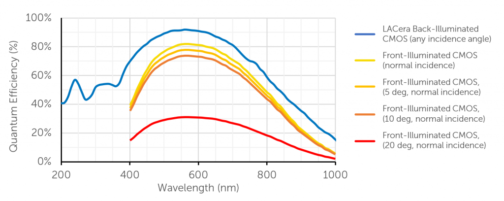
The result is a sensor with a near-perfect 90+% QE at the peak. However, due to the greater challenges to manufacture back-illuminated CMOS devices, back-illumination only came to scientific-grade CMOS cameras in 2016. Compared to front-illumination, back-illumination results in a 10-15% QE increase across the standard 400-1100 nm field, even unlocking additional wavelengths less than 400 nm. Further, back-illumination also removes the dependence of the QE upon the angle of incidence.
The Challenge of Back-Illuminated Global Shutter CMOS
How is Global Shutter achieved on CMOS?
Whether a CMOS camera has a rolling shutter or a global shutter, the process of reading the signals happens row-by-row, as each row is passed to that column’s Analogue to Digital Converter (ADC) to be measured. For rolling shutter cameras, the readout for a row happens immediately after the end of the exposure of the row, moving on to the next row once readout is complete. To achieve a global shutter, exposure must start and end simultaneously, with readout happening after all pixels are exposed. In this case the exposure is ended through simultaneously moving each pixel’s acquired photoelectrons into a storage area in the pixel. The exposure and readout sequence then is the following:
- Begin exposure for all rows simultaneously by resetting the charges stored in the pixel (the photodiode), and the storage (called the floating diffusion, FD).
- Photons are then collected for the specified exposure time
- End the exposure of the image formed by moving the acquired photoelectrons into the storage area within each pixel, where they await readout.
- Row by row, read the voltage corresponding to each pixel from the floating diffusion.
- Reset the floating diffusion’s voltage to the default ‘bias’ value, and measure this once again to give a more accurate baseline for the signal. Repeat for the next row.
- Repeat this sequence for each frame
Parasitic Light Sensitivity
The Floating Diffusion (FD) where charge is stored before readout is in fact light-sensitive, meaning if photons reach this area after the end of an exposure but before the readout process occurs for that pixel, anomalous signal can be recorded. This is known as ‘parasitic’ light sensitivity (PLS). This is defined as:
For front-illuminated devices, the FD is hidden under the wiring that blocks incoming photons. In this case, the FD is exposed to very few photons, with only a small number being deflected into the FD by the microlenses of the camera.
For back-illuminated devices however, global shutter acquisition without appreciable PLS was previously impossible for scientific cameras, as the rearrangement of the pixel to allow greater sensitivity also exposed the FD to light. PLS could effectively introduce rolling shutter artifacts into global shutter images, and lead to uneven exposure to light across the frame. For precise scientific imaging applications, despite the advantages of back-illumination for sensitivity, PLS previously ruled out the use of global shutter sensor architecture.
LACera Technology: Achieving Back-Illuminated Global Shutter CMOS
To bring together the unmatched sensitivity of back-illuminated CMOS and the distortion-free images of Global Shutter would require a fundamental redesign of components of the sensor. At Teledyne, we were able to leverage our influence over the sensor production process for LACera technology to optimize the pixel geometry and significantly reduce the possibility of parasitic light capture.
Through this innovation, sensitivity and optimum sensor behavior are united in a single scientific-grade sensor technology for the first time. For applications requiring high-speed, low-light or distortion-free images, LACera technology opens the door to CMOS technology and all the improvements it brings for scientific imaging.
LACera represents a critical element of advanced imaging solutions and is only possible with the nature and scale of Teledyne. From pixel, sensor, and ROIC design, through low noise electronics, to deep cooling, and system interface, Teledyne is the only company capable of delivering this one hundred percent organic solution in large-format CMOS.
Conclusions
With LACera technology, there is no longer any compromise between maximizing sensitivity through light collection and the ability to capture images at high speed free of rolling shutter artifacts, essential for many applications.
Further Reading
New Era in Dynamic Range and Linearity
Find out more about how innovations in the CMOS readout process now offers unsurpassed dynamic range and linearity.

Cooling in Large-Area CMOS
Find out more about the deep cooling of LACera Technology, resulting in low dark current with ultimate reliability and cooling performance.

Request a Technology Discussion
Teledyne Imaging is soliciting commercial partnerships. If your organization is interested in learning more please request a technology discussion.