
Researchers: Samuel Berweger and Prof. Markus Raschke – Department of
Physics, Department of Chemistry, and JILA, University of Colorado at Boulder
Background
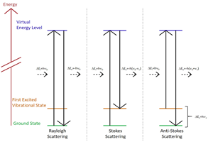
The ability to identify small quantities of adsorbed analyte or structural features down to the few-molecule level is a key challenge in nanotechnology. Optical spectroscopy provides an attractive means to achieve such identification via non-invasive implementations and the potential for chemical sensitivity. Raman scattering has emerged as a particularly powerful technique due to its capability for nondestructive vibrational fingerprinting using only monochromatic visible light sources; unfortunately, this method suffers from weak signal levels, preventing the study of small quantities of molecules or other structures.
Enhancement of the optical electric field as necessary to improve Raman signal levels can be achieved by utilizing localized plasmon resonances in noble metal nanoparticles. These resonances, which result from localized charge density oscillations, can yield a Raman enhancement of up to 10 orders of magnitude via the surface-enhanced Raman scattering (SERS) effect1. In conventional SERS, however, the enhancement can be difficult to control and remains spatially confined to stationary nanoparticles or surface features.
To obtain a microscopy technique based on the same general principle, tip-enhanced Raman scattering (TERS) can be implemented as a scanning probe method, providing optical nanometer spatial resolution. Here, rather than relying on the field enhancement of stationary nanoparticles, a plasmon resonance located at the apex of a noble metal scanning probe tip is utilized. The inherent flexibility of a scanning probe system affords the freedom for spatially resolved spectroscopic probing and imaging of surface analytes.
By virtue of the ultrahigh optical spatial resolution2 resulting from the spatial confinement of the near-field of the apex plasmon, combined with enhanced sensitivity, TERS has been utilized to study a variety of systems. Using dyes deposited onto metallic substrates as model systems, single-molecule sensitivity has been demonstrated3-5. Other systems have included biologically relevant molecules and systems6-7, cells8, and materials of reduced dimensionality, such as graphene and carbon nanotubes9.
Furthermore, as a spectroscopic tool of fundamental importance to the investigation of solid-state systems, TERS has been used to study crystalline systems ranging from semiconductors10 to ferroelectrics. In particular, the intrinsic symmetry of tensor-based Raman selection rules in combination with the polarization dependent tip enhancement has enabled the imaging of ferroelectric domains in perovskite BaTiO311.
Setup
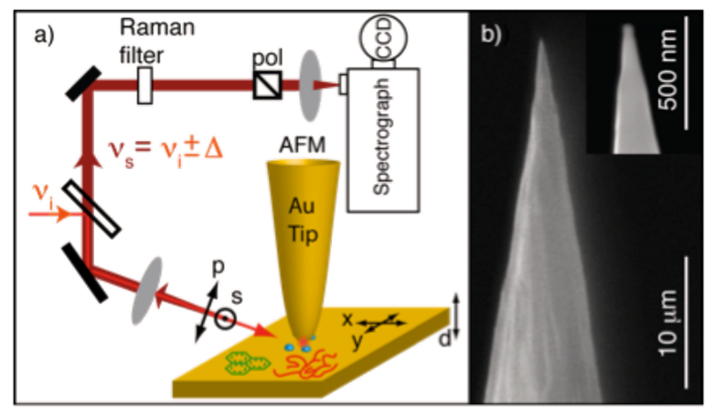
A schematic of the experimental setup utilized by the Raschke group at the University of Colorado is shown in Figure 1(a). The illumination wavelength should be chosen to match the plasmon resonance position of the tip apex. The plasmon resonance is spectrally broad (~100 nm) for the geometries obtained by electrochemical etching; Au tips often exhibit plasmon resonances in the 600 – 800 nm range. However, empirical tip selection by trial and error must be performed to select a suitable tip for, as an example, the frequently used 632.8 nm HeNe laser line.
Furthermore, TERS and SERS both experience Raman enhancement not only via the amplification of the incident light, but via the Raman scattered light, which is enhanced as well, with the relative amplitudes of the enhancement being related to the strength of the plasmon at the spectral position of both the excitation and Raman emission wavelengths12. As a consequence, it is usually desirable to utilize an excitation wavelength relative to the tip apex plasmon spectrum such that the enhancement is high at both the excitation and Raman-scattered wavelengths. Due to the ∞mm symmetry of the tip, the field enhancement is polarization dependent and maximum for tip-parallel polarizations.
The TERS light can be collected with the same objective in a backscattering geometry in which it passes a beamsplitter, is spectrally filtered using a Raman edge filter, and detected using an imaging spectrograph with a liquid nitrogen-cooled CCD camera. In order to measure low signal levels requiring long acquisition times and to reduce imaging aberrations, the Raschke group utilizes an Acton Series SP-500i in combination with a Spec-10 camera (1340 x 100 pixel array), both from Princeton Instruments. Direct confocal imaging of the tip apex onto the entrance slit of the spectrometer is preferred over the use of intermediate fiber coupling with its unavoidable losses and additional alignment uncertainties.
The need for accurate tip-sample distance control and sample scanning requires the use of a scanning probe microscope: generally either a scanning tunneling microscope (STM) or an atomic force microscope (AFM). Scanning tunneling microscopy provides the ability to control a tip a few nanometers above a surface, but the necessity for conductive samples renders it unsuitable for many TERS applications. Atomic force microscopy, meanwhile, is highly effective for studying nonconductive samples.
Commonly used AFM tapping and noncontact modes utilize high dither amplitudes though, resulting in a smaller time-averaged field enhancement near the sample surface. Therefore, AFM contact or shear-force modes are frequently used instead. In particular, shear-force mode maintains the tip at a constant height of a few nanometers above the sample surface, thus preventing tip damage, while small lateral dither amplitudes do not compromise the spatial resolution. The Raschke group utilizes shear-force feedback in their home-built system.
As noble metal tips are not yet commercially available, the Raschke group fabricates Au tips via an electrochemical etching procedure13. The resultant tips have a smooth surface and uniform taper, as shown in Figure 1(b), with tip apex radii on the order of tens of nanometers, reproducibly achievable using an electronic cut-off circuit to terminate the etching process. Alternately, thermal vapor deposition of noble metals onto commercial AFM tips can result in TERS-active tips.
TERS
Associated with the high field enhancement is a spatial confinement of the near-field surrounding the TERS tip, allowing optical spatial resolution down to ~10 nm. The spatial extent of the near-field becomes apparent in Figure 2(a), which shows TERS spectra acquired for decreasing separations between the tip and a monolayer of the dye Malachite Green deposited onto a Au substrate. For tip-sample distances greater than 30 nm only, a far-field background signal is observed. For shorter separations, however, an increase in the signal is seen for decreasing distances, correlated with the spatial extent of the enhanced near-field and the tip apex radius. From TERS spectra acquired with the tip in shear-force feedback, the characteristic peaks of Malachite Green are seen, as shown in Figure 2(b), as well as a broad luminescence background resulting from the resonant Raman excitation.
In this case, from the near- to far-field Raman contrast, one can estimate a Raman enhancement of >105, while values of >108 are achievable12. The increased sensitivity associated with this field enhancement in combination with the unique Raman spectrum allows, in principle, the identification of surface adsorbates or other features. Furthermore, with the ability to probe molecular vibrations or crystal phonons with nanometer spatial resolution and imaging capabilities, tip-enhanced Raman scattering is not only a powerful analytical technique but a powerful tool for fundamental solid-state research.
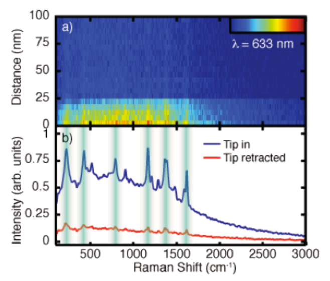
It should be noted, however, that the far-field background signal seen in Figure 2 is frequently observed in TERS experiments. Originating from the diffraction-limited excitation focus, this background can be reduced via careful experimental consideration. Nonetheless, it is often present and can overpower the desired near-field signal and lead to signal artifacts.
In ongoing work, the Raschke group is exploring means for improving the versatility and applicability of TERS. To this end, the group has been developing the grating coupling of surface plasmon polaritons onto the shaft of electrochemically etched Au tips for adiabatic nanofocusing14-15. As the resultant nanometer spatially confined excitation at the tip apex is generated nonlocally, the spatial separation of the incident light at the grating from the apexlocalized excitation eliminates the primary pathway by which far-field background is generated in TERS.
At longer wavelengths, this background-free TERS also yields highly improved focusing efficiency, allowing TERS in the near-IR despite the 1/λ4 dependence of Raman scattering. Highly efficient spectrometers and CCD cameras, such as the Acton Series LS-785 lensbased imaging spectrograph16 and the PyLoN:100BR_eXcelon cryogenically cooled CCD camera from Princeton Instruments, enable detection of the weak signals.
The significantly improved background suppression will enable the study of large or bulk structures, where the far-field background is typically strong in conventional TERS. In addition, the ability to deliver energy to a nanoconfined excitation will find applications not only in TERS but in the localized control of surface plasmons and ultrafast pulses.
Resources
For more information about the Raschke group in the Department of Physics at the University of Colorado, please visit: http://nano-optics.colorado.edu/index.php?id=3
References
- Nie, S. and S.R. Emory, Probing single molecules and single nanoparticles by surfaceenhanced Raman scattering. Science, 1997. 275: p. 1102.
- Yano, T., et al., Pressure-assisted tip-enhanced Raman imaging at a resolution of a few nanometres. Nat. Photonics, 2009. 3: p. 473.
- Neacsu, C.C., et al., Scanning-probe Raman spectroscopy with single-molecule sensitivity. Phys. Rev. B, 2006. 73(19): p. 193406.
- Steidtner, J. and B. Pettinger, Tip-enhanced Raman spectroscopy and microscopy on single dye molecule with 15 nm resolution. Phys. Rev. Lett., 2008. 100: p. 236101.
- Zhang, W., et al., Single molecule tip-enhanced Raman spectroscopy with silver tips. J. Phys. Chem. C, 2007. 111: p. 1733.
- Bailo, E. and V. Deckert, Tip-enhanced Raman spectroscopy of single RNA strands: towards a novel direct-sequencing method. Ang. Chem. Int. Ed., 2008. 47: p. 1658.
- Schmid, T., et al., Towards chemical analysis of nanostructures in biofilms II: tip-enhanced Raman spectroscopy of alginates. Anal. Bioanal. Chem., 2008. 391: p. 1907.
- Cialla, D., et al., Raman to the limit: tip-enhanced Raman spectroscopic investigations of a single tobacco mosaic virus. J. Raman Spectrosc., 2009. 40: p. 240.
- Hartschuh, A., et al., High-resolution near-field Raman microscopy of single-walled carbon nanotubes. Phys. Rev. Lett., 2003. 90(9): p. 095503.
- Hayazawa, N., et al., Visualization of localized strain of a crystalline thin layer at the nanoscale by tip-enhanced Raman spectroscopy and microscopy. J. Raman Spectrosc., 2007. 38: p. 684.
- Berweger, S., et al., Optical nanocrystallography with tip-enhanced phonon Raman spectroscopy. Nat. Nanotechnology, 2009. 4: p. 496.
- Le Ru, E.C., et al., Experimental verification of the SERS electromagnetic model beyond the |E|^4 approximation: polarization effects. J. Phys. Chem. C, 2008. 112: p. 8117.
- Ren, B., G. Picardi, and B. Pettinger, Preparation of gold tips suitable for tip-enhanced Raman spectroscopy and light emission by electrochemical etching. Rev. Sci. Instr., 2004. 75: p. 837.
- Neacsu, C.C., et al., Near-field localization in plasmonic superfocusing: a nanoemitter on a tip. Nano Lett., 2010. 10: p. 592.
- Ropers, C., et al., Grating-coupling of surface plasmons onto metallic tips: a nanoconfined light source. Nano Lett., 2007. 7(9): p. 2784.
- Berweger, S., et al., Adiabatic tip-plasmon focusing for nano-Raman spectroscopy. J. Phys. Chem. Lett., 2010. 1: p. 3427.
Further Reading
Introduction to Raman Spectroscopy
Introduction into how Raman spectroscopy occurs, what it can be used to measure, and how it can be used within internal and environmental sensing.
Raman Spectroscopy in Life Sciences
Brief overview of how Raman spectroscopy is advantageous for life science applications, such as characterizing biomolecules and for biosensing.
Related Raman Products
Raman spectroscopy can be implemented in various ways dependent on the sample being studied. Therefore it is important to use the correct equipment. Find out more about your options here.